Quantcast
Channel: KA7OEI's blog
Viewing all 197 articles
Browse latest View live

"TDOA" direction finder systems - Part 1 - how they work, and a few examples.

$
0
0
Next to using a directional antenna, one of the simpler ways to determine the direction of a received signal is to use what is often referred to as the "TDOA" system which stands for Timed Direction Of Arrival.

One method of implementation involves the use of two separate antennas, switched at an audible rate, and connected to a narrowband FM receiver.  In its simplest form the antenna switch signal could be produced by anything from a 555 timer to an oscillator made from logic gates to one made using an op-amp:  All that is necessary is that the duty cycle of the driving (square) waveform me "near-ish" 50% (+/- 30% is probably ok...) and be of sufficient level to adequately drive the switching diodes on the antenna.

See the diagram below for an explanation of how this system works:
Figure 1:
A diagram showing how the "TDOA" system works.
Click on the image for a larger version.

In short, if both antennas - which are typically half-wave dipoles - are exactly the same distance from the signal source, the RF waveform on each of the two antennas will have arrived at exactly the same time.  If we electronically switch between the two antennas, nothing will happen because both signals are identical.

If one of the two dipoles in our DF antenna is closer to the transmitter than the other, switching the between the two antennas will cause the receiver to see a "jump" in the RF waveform:  Switching from, say, A to B will cause it to jump forward while switching from B to A will cause it to switch backward.

The switching, causing the RF waveform to "jump", is seen by the FM receiver as phase shift in the received signal - and being an FM receiver, it detects this as a "glitch" in the audio as depicted in Figure 2:
 
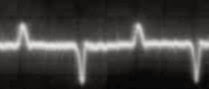
Figure 2:
Example of the "glitches" seen on the audio of a receiver connected to a TDOA system that switches antennas.

Because the discontinuity in the RF waveform caused by the antenna switch is abrupt, the "glitch" in the audio waveform is transient and occurring only when the antenna is switched.  You might notice something else in Figure 2 as well:  If we assume that a the first glitch is from switching from antenna "A" to antenna "B" and that it causes the glitch to be positive-going,  the switch from antenna "B" back to antenna "A" is going to be negative-going. Ideally, the glitches are going to be equal and opposite but sometimes - such as the case in Figure 2, they are not exactly the same and this is usually due to multipath distortion at the DF antenna array.

At this point, several things may have already occurred to you:
  • If switching from antenna "A" to antenna "B" causes a positive glitch and vice-versa, we know that the antenna array is not broadside to the transmitter.
  • If we rotate the antenna so that switching from antenna "B" to antenna "A" now causes a positive glitch and from "B" to "A" causes a negative one, we can reasonably assume that if antenna "A" were closer to the transmitter before we rotated it, that the direction of the transmitter is somewhere in between the two antenna positions.
  • If the two antennas are equidistant from the transmitter, the glitches will go away entirely.  At this point, the antenna will be oriented directly broadside to the transmitter, indicating its bearing.
  • The magnitude of the glitches provides some indication of the error in pointing:  If the antennas are equidistant with the two-element array perfectly broadside to the transmitter, the amplitude of the glitches will be pretty much nonexistent, but if the antenna is 90 degrees off (e.g. with the boom "pointed" at the transmitter as one would a normal Yagi antenna) the glitches - and the audible tone - will be at the highest possible amplitude.
Detecting the glitches by ear:

If the antennas are switched at an audible rate, these glitches will be clearly audible as a tone superimposed on the received signal.  While it is not possible to determine the phase relationships of these glitches by ear to determine whether the transmitter is to the left or right of our signal, by sweeping it back and forth and mentally noting where the "null"(e.g. the point at which the tone disappears) is, we can infer the direction of the transmitter by doing so - and that is exactly how the simplest of these TDOA systems work.

For an example of a simple TDOA system using a 555 timer, see the following web page:

WB2HOL 555 Time Difference-of-Arrival RDF - link

This circuit is about as simple as it gets:  A 555 timer that generates a square-ish wave.  It is up to the user to move the antenna back and forth, note the null and infer from that the direction of the signal.

It should be noted that in this case the transmitter could be behind the user, but with a bit of skill and practice one can resolve this 180 degree ambiguity - particularly if one is fairly close to the transmitter - by noting how the apparent bearing changes with respect to the relative locations of the user and the transmitter.

Detecting the glitches electronically:


To electronically determine if the signal is to the left or right of our position we must be able to determine if the glitch that occurs when switching from on antenna to the other is positive-going or negative-going and to do this, we need some simple circuity and one way to do this is to include a "window" detector - that is, a detector that "looks" at the receive audio for a brief instant, just after the antenna switch occurs and here are two circuits that do just that:

WB2HOL's Simple Time Difference-of-Arrival RDF - link
and
The WA7ARK TDOA units - link  (Some of the circuits on this page are described below. )

In looking at the WA7ARK pages, we find two units that indicate left/right in different ways:
  1. In the "Aural" unit, a 565 chip - which is a PLL (Phase Locked Loop) - is used to both generate the signal for switching the antennas and also to determine if the signal indicated is to the left or right by changing the pitch of the tone.
  2. In the "Metered" unit described below, an approach is taken very similar to that of the WB2HOL Simple Time Difference-of-Arrival RDF circuit in that a "snapshot" of the audio is taken an the appropriate time to determine the polarity of the glitches and display this as a left/right indication on a meter movement.
In both of these circuits one still hears the tone, but there is an additional input to the user - the pitch of the tone in the case of #1 and the movement of the meter for #2 - to indicate that the transmitter is left/right of the current antenna orientation.  Having this additional information also helps the user more-easily resolve the 180 degree ambiguity because, if the transmitter is behind, the left-right indications will be reversed.

Finding the glitches:

At this point in the discussion I would like to redirect your attention back to Figure 2, above.  You'll notice that these glitches are really quite brief:  They don't last very long at all - and most of the space between glitches is empty - at least if there is no other audio on the transmitted signal.

What about if the signal being received is heavily modulated with voice or noise?  That glitch can be easily lost amongst the clutter - but we have advantage:  We can know precisely when that glitch is going to occur and look for it only then, ignoring everything else.  In selectively looking for that glitch, much of the effect of modulation on that signal that would serve to "dilute" the signal that we want is reduced and this method is used in the "Metered" version of the WA7ARK circuit, reproduced below:
Figure 3:  The WA7ARK "Metered" circuit.
The "X" and "Y" taps are always "5" apart (0 and 5, 2 and 7, etc.) and are selected either with an oscilloscope or
experimentally, using a "clean" signal from a known-good receiver.
Click on the image for a larger version.
This circuit works as follows:
  • U3C, an op amp, is wired as an oscillator with the frequency selected as being in the neighborhood of 10 kHz.  The precise frequency really isn't critical, but it should be stable:  Just make sure that you don't use a ceramic capacitor for C4.
  • U2 is a 4017 CMOS divide-by-10 counter.  The "Cout" pin has a square wave at 1/10th of the frequency of the U3C oscillator (approximately 1 kHz) and this signal, buffered by U3D, drives the switched antennas.
  • The FM receiver is connected via J1 and this contains the audio with the "glitches" in it.
  • For every 10 count made by U2, there are two glitches:  One occurs when the square wave output from U3D goes from high-to-low, and another when it goes from low-to-high.  During that time, the "0-9" outputs of U2 go high, one-at-a-time, representing each of its 10 counts and is high for only 10% of the total time.
  • As shown in the diagram, we select two of the 0-9 outputs of U2, 5 counts apart from each other.  We pick the output that goes high at the same instant that the "glitch" from the receiver's audio arrives.
  • Being driven by U2, U1 contains electronic switches that are activated by the two, brief signals from U2 that we have selected to go high when the glitches arrive.  When activated, the appropriate switch inside U1 is closed at a time that coincides with the glitch and this brief signal changes the charges on C2 and C3, the voltage correlating with both the amplitude and polarity of the glitch.
  • U3A and U3B buffer the voltages on C2 and C3 and feed it to a zero-centered meter:  The more the charges on C2 and C3 differ from each other, the more the meter swings away from the center.  Since the voltages on C2 and C3 are derived from the glitches that occur, the meter indication tells us not only whether the signal is to the left or right of us, but also something about how far to the left/right it is!
By using a "windowed" detector driven by the relatively brief pulses from U2, we are only looking at our receive audio for 2/10ths of the time (e.g. 20%) and ignoring what is happening during the other 80% of the time and since our meter is connected across these two points it is also only going to react to energy that is consistently "equal and opposite" - as that of the "glitches" depicted in Figure 2.

Because we are looking at only the 20% of the time during which a glitch is coming in, we not only better-reject other audio that might be being transmitted on that signal, but by virtue of some filtering provided by capacitors C2, C3 and resistor R3, we are averaging out the noise and other modulation as well, further improving our effective sensitivity and reducing our susceptibility to effects of noise and modulation on our received signal!

In actual use, one would determine the optimal taps for "X" and "Y" on U2 in the diagram above - either with an oscilloscope, or experimentally by adjusting the taps using a clean tone - no modulation received using an antenna like that described below for the highest meter indication.  For calibration, one would simply set the volume on the receiver to cause full-scale deflection when the antenna was pointing "away"(e.g. 90 degrees rotated from the two elements being broadside to the transmitted signal).  If necessary, you may make R4 variable, placing a 1k resistor in series with a 10k-25k potentiometer.

The antenna:

Up to this point the antenna has been mentioned only in passing.  The simplest antenna - and one that works well for practically any of the simple TDOA systems (of the "left/right" variety) you are likely to find - is depicted below:
Figure 4:
A typical TDOA switch antenna.
The only critical points are that dimensions "L2" and "L3" be equal to each other and cut according
to the lengths calculated using the notes on the drawing above or using the example below.
Click on the image for a larger version.
Note:  The antennas depicted on the WB2HOL pages, linked above, will also work.

While the antenna depicted in Figure 4looks like a 2-element Yagi, it is not.  What's more, it is important to realize that while you would line up the elements of a Yagi to point it at the signal being sought, this antenna - when "pointed" toward the transmitter - will have its elements oriented broadside to the transmitter.  In other words, if you are facing the transmitter and you are holding the antenna centered in front of you, one of its elements will be to your right and the other will be at the same distance, but on your left.


A few notes about construction:
  • The two elements must not be spaced farther than 1/2 wavelength apart at the highest frequency for which you plan to use the antenna.  If they are spaced farther than 1/2 wavelength apart, you'll get nonsensical readings!  Spacing them about 1/4 wavelength apart on 2 meters (144 MHz) results in a fairly compact and manageable antenna.
  • Make sure that the two pieces of coax depicted by "L2" are of the same type and length - an electrical 1/2 wavelength apart:  Note that the "velocity factor" of coax will mean that the coax's physical length will be significantly shorter than its electrical length.
  • For D1 and D2, use identical diodes.  Preferably, a PIN switching diode will work, but a 1N914 or 1N4148 will work in a pinch with somewhat degraded performance.  Reportedly, 1N4007 diodes (the 1000 volt version in the 1N400x family of diodes) work fairly well on 2 meters for this purpose.
  • For 2 meters, typical values might be:
    • L1 = 16 inches (42cm)
    • L2 = 13.5 inches (34cm) for cable with a solid polyethylene dielectric.
    • L3 = 38 inches (97cm) total consisting of two pieces of half that length. 
 How the antenna switching works:

If you look at Figure 3 you will see J2, which is connected to the DF antenna and J3, which is connected to the receiver and separating the two is C7, a 47pF capacitor:  C7 is too small to effectively pass our audio-frequency antenna switching signal and is thus able to prevent it from entering the front end of our receiver.

Our switching signal - a square wave - is coupled to the antenna via C6 and this capacitor is large enough that it allows the square wave to pass, but since it is AC coupled, it causes our positive-going square wave from U3D to become bipolar, centered about zero going both positive and negative with respect to ground.  R9 is used not only to limit the level of the square wave being fed to the diodes, but it also isolates the RF signal present at J2/C7 from the rest of the circuit.

The now-bipolar square wave travels down the coax to our antenna along with the RF and when it is positive-going, D1 (in Figure 4) conducts and reverse-biases D2, shutting it off, but when it is negative-going, D2 conducts and D1 is reverse-biased:  It is only when a diode is conducting that it is transparent to RF and in this way, we can alternately select either the left or the right element.

When using the antenna:
  • The above antenna only works well for vertically-polarized signals since the antenna must be held with the elements vertical to get left/right indications.
  • Remember that you do NOT use this as you would a Yagi.  The tone will disappear when the elements are vertical and the plane of the two elements are broadside to the distant transmitter.  In other words, if you are holding the antenna up to your chest, one element will be near your left arm and the other will be near your right.
  • If you "point" the boom at the transmitted signal as if it were a normal Yagi, you will get the loudest tone.
  • Because this is FM - and with FM, signal strength doesn't matter once the signal is full-quieting - the loudness of the tone will tell you nothing about the strength of the received signal.  Again, the loudest tone indicates that the antenna is about 90 degrees off the bearing of the transmitter and the tone disappearing tells you that the antenna is perfectly oriented broadside to the transmitter.
  • Remember that if the transmitter is behind you, the left-right indications (if the unit has the capability) will become reversed.
  • The presence of multipath and reflections can easily confuse a system like this.  Remember to note the trend of the bearings that you are getting rather than relying on a single bearing that might suddenly indicate a wildly different different direction:  If you do get vastly different reading, move to a different location and re-check.  Unless you are very near the transmitter - which probably means that you can disconnect the antenna cable from the radio and still hear the transmitter - a small change in location should not cause a large change in bearing:  If it does, suspect a reflection.

A few comments about some inexpensive imported radios and their suitability for use with these types of circuits:

In recent years there are a number of very inexpensive radios - mostly with Chinese names - that have appeared on the market in the sub-$100 price range - some $50 or below - and the question arises:  Are these suitable of direction-finding?

The quick answer is "possibly not."

Many of these radios use an "all-in-one" receiver chip which has several issues:
  • These radios tend to overload very easily in the presence of strong signals.  If one is very close to the transmitter being sought they can do strange things such as experiencing phase shifts.  If one is attempting to use one of these radios with an "Offset Mixer"(a different article...) then it can simply become impossible!
  • Many of these radios also have an audio filter that kicks in when the signal is weak and noisy that cannot be disabled.  This low-pass filter - which is apparent when the hiss or audio suddenly sounds somewhat muffled - causes a different audio delay.  While this will likely have little effect with the simplest TDOA circuit where one is simply listening to a tone, it will likely "break" fancier ones that provide left-right indications.
If you have one of these inexpensive radios and can't seem to make the circuit work, try a different radio - preferably one from one of the mainstream amateur radio brands - during your troubleshooting!


In the next part - to be posted some time in the future - we'll talk about how one might implement what we have learned about the circuits, above, in software.


On the winding of power chokes and transformers: Part 2 - A filament transformer

$
0
0
Having wound the choke described in the previous installment about chokes - (link)- I decided to proceed with the next logical step in the project:  Winding a filament transformer.
Figure 1:
The completed filament transformer, before varnishing,
ready for testing.
Click on the image for a larger version.

With the lower voltage requirements, the filament transformer is the next-easiest since being a step down transformer, fewer turns are required overall and the wire sizes will be larger.

The first step was to figure out my voltage and current requirements - but this was already known in the form of the filament requirements of the tubes to be used:  Two center-tapped windings, each capable of 11 volts at 11 amps.  To calculate the necessary winding parameters (e.g. number of turns, size of wire, etc.) I will refer again to the two links noted in the previous installment, included below:

  1. Turner Audio(link) - These pages contain much practical advice on power and audio transformers and chokes.  (Refer to the link "Power Transformers and Chokes" (link) and related pages linked from that page.)
  2. Homo-Ludens - Practical transformer winding(link) - While mostly about power transformers, this page also contain practical advice based on hands-on experience of winding, re-winding and reverse-engineering/rebuilding transformers.  There is also another linked page "Transformers and Coils"(link) that has additional information on this topic.
While there are enough equations and general information spread across both pages to provide the necessary information if you want to crunch numbers with equations, of particular interest is a spreadsheet found on the Homo-Ludens "Practical transformer winding" web page that allows one to "play" with various configurations.  For this spreadsheet we will need to input what we already know, such as:
  • Input voltage:  120 VAC (nominal) at 60 Hz.  Since we want to have multiple taps to fine-tune the voltage, we'll also calculate for 115 and 125 volts.
  • Output voltage:  11 amps under load.  A rule of thumb is to add 5% to this to accommodate various losses so this would be (11 * 1.05 = 11.025) or approximately 11.5 volts.
  • Output current:  22 amps - the total sum of the two 11 amp filament windings.  They will be "split" in later calculations.
  • Core size:  E150.  The Edcor core and bobbin that will be used has a stack height of 38mm and a center leg that is 38mm across.
  • Set a design goal for wire sizes corresponding with a current density of 0.4 mm2/amp, a rather conservative number.
  • Let us initially set a "fill factor" of 0.4 - more on this parameter, later.
  • Core material information:  The Edcor laminations use M-6 GOSS (Grain-Oriented Silicon Steel) which is a material that is capable of safely handling higher magnetic flux than "generic" iron cores.  This has two important implications:
    • The saturation flux of this material is in the area of 1.7 Tesla.  This is a very "soft" number, dependent largely on how much core heating one is able to tolerate in the intended application.
    • The iron loss (in watts/kg at 1 Tesla) for the M-6 material is quite low - approximately 0.5 watts/kg@1T (at 50 Hz) versus 2 watts/kg@1T for "generic" transform iron.  The spreadsheet expects a 50 Hz value here regardless of the actual frequency.
A few words about the wire size:

The value of 0.4mm2/amp target that I chose is fairly conservative based on the recommendations found in several sources:
  • The Turner Audio site suggests a value of (3 amps/mm2) = 0.33mm2/amp as a general number.
  • The Homo-Ludens site suggests a value of 0.35mm2/amp for "medium-sized" transformers (50-300 watts) wire such as this and smaller/heavier (0.25 and 0.5mm2/amp)conductors for very small and large transformers, respectively.
  • Various vintages of the ARRL Amateur Radio Handbook note that a value of 1000 cma (0.506mm2/amp) as being "conservative" with a value of 700 cma (0.354mm2/amp) being suggested.
  • Interestingly, the 1936 Jones Radio Handbook notes recommends a 1000 cma
    (0.506mm2/amp) value for typical amateur use and increasing this to 1500 cma (0.759mm2/amp) for transformers that would be intermittently subjected to significant overload and/or were in hot, poorly ventilated environments.  These recommendations are understandably based on the use of older materials such as paper insulation and the more fragile varnished/enameled wire of the day.
  • If one peruses the Edcor site one can glean bits of data here and there and they mention a design goal of 500 cma (circular-mill amperes) which converts to 0.253mm2/amp.  (Reference:  Tek Note 43 - link.)  When I read this I presumed that this recommendation may have been intended for small, low-power transformers, but I notedthis posting - link in their forum where a current of 200mA is mentioned being used with 30 AWG wire which calculates to 0.254mm2/amp.
Even more about flux density:
  • As noted, for inexpensive, generic cores of unknown properties Turner Audio suggests a maximum flux of 0.9 Telsa while the Homo-Ludens site suggests that 1.0 Tesla is "probably OK" for the vast majority of cores of unknown provenance.  The later site recommends that if these cores are being re-used that one counts the number of turns on the original primary (if it is being re-wound) and use this, along with the core's cross-sectional size to estimate the original flux density.
    • Comment:  If you are keeping the original primary winding, one would wind a few dozen turns of hookup wire and carefully measure the resulting, unloaded voltage.  Comparing this with the applied primary voltage and taking the number of temporary turns that one wound the number of turns on the primary could be quite accurately determined.
  • The M-6 material is capable of much better performance than "generic" iron - likely being usable at 1.6-1.7 Tesla, but Edcor mentions in Tek Note 43 (linked above) that their design goal is 1.4 Tesla - value with which both the Turner Audio and Homo-Ludens sites agree as being appropriate for this material.  Based on typical curves for M-6 material, this would seem to be a reasonable compromise between higher core losses, fewer turns (e.g. higher flux) and more turns with higher copper losses, lower core losses (lower flux).
 Based on the above I decided to use 1.4 Tesla in my design.
    Crunching the numbers:

    Inputting the above to the spreadsheet one can see that it does not actually care about the output current, but rather is tells you the highest possible load current and volt-amp capacity based on the core size and flux density that you specify and the most important information that it gives is the number of turns for the primary:  It is up to you to scale back the "worst case" numbers that it gives you to better suit your needs and make sure that everything will fit in the available space.

    For example, given the information that we already have, the spreadsheet calculates that with the entered parameters one could expect to pull well over 26 amps at 11.5 watts - about 292 volt-amps using the wire targets along with what is calculated to be able to fit given the calculated wire sizes and the inputted fill factor.  In reality, we will need closer to (11.5 volt * 22 amps =) 253 volt-amps so we would be safe in downsizing our wire to about 83% of the calculated cross-sectional area.  Assuming the worst case loading of the primary - which occurs at the lowest primary voltage, 115 VAC, we can calculate that our maximum primary current will be (253 volt-amps / 115 volts) = 2.2 amps.
    • If we consult a wire table to see which size most closely matches our 0.4mm2/amp criteria (e.g. 0.4mm2/amp * 2.2 amps = 0.84mm2) we find:
      • 17 AWG wire at 1.04mm2.  This is (1.04mm2 /amp / 2.2 amps) = 0.472 mm2.
      • 18 AWG wire at 0.823mm2.  This is (0.823mm2/amp / 2.2 amps) = 0.37 mm2.
      • 19 AWG wire at 0.653mm2.  This is (0.653mm2/amp / 2.2 amps) = 0.30 mm2.
    As we can see, either 17 or 18 AWG would be fine for the primary, both sizes being quite close to our design goal:  17 AWG will run a bit cooler with lower loss while 18 AWG will take up a bit less space on the bobbin.  19 AWG does fit within the Edcor guidelines but is much smaller than target - but would still probably be OK if one tolerated a bit of extra heat and voltage drop.

    Based on the 1.4 Tesla flux values we can see that at 115 Volts we would need 223 turns on our primary to achieve the target of 11.5 volts and since the ratio of primary-secondary turns is exactly the same as our voltage ratio, we can calculate:
    • 115 volts / 11.5 volts = 10:1 ratio
    What this means is that for our 223 turns on the 11.5 volt primary, we would need (223 / 10) = 22.3 turns.  Since it is awkward to wind a fractional turn, let's round down to 22 turns - an even number that also makes it easy to locate the center tap point.  By increasing the number of turns slightly we must now recalculate the 115 volt primary winding using the same ratio as above:
    • Doing this, we will need (10 * 22) = 220 turns.  This reduction in turns from 223 increases the flux density on the core, but only by a few percent so we can ignore it.
    Let us now calculate the number of turns for 120 and 125 volts:
    • 120 volts / 11.5 volts = 10.435:1 ratio.  22 turns * 10.435 = 229 turns, rounded down.
    • 125 volts / 11.5 volts = 10.870:1 ratio.  22 turns * 10.870 = 239 turns, rounded down.
    Since we need two filament windings, each capable of of 11 amps, we calculate the appropriate wire size for each:
    • For 11 amps, we calculated a minimum wire cross-sectional area of (0.4 mm2/amp * 11 amps) = 4.4 mm2.  Consulting the table, we find:
      • 10 AWG wire at 5.26mm2.  This is (5.26mm2/amp / 11 amps) = 0.48 mm2
      • 11 AWG wire at 4.17mm2.  This is (4.17mm2/amp / 11 amps) = 0.38 mm2
      • 12 AWG wire at 3.31mm2.  This is (3.31mm2/amp / 11 amps) = 0.30 mm2
      • 13 AWG wire at 2.62mm2.  This is (2.62mm2/amp / 11 amps) = 0.23 mm2
    From all of the above we can see the 11 AWG wire is very close to our 0.4mm2/amp target - and still above the recommendations of the two web sites listed above while 12 AWG appears to be suitable if one goes with the Edcor guidelines.  It should also be noted that because these primary windings are on the "outside" layer (the reason to be noted later) they can more readily dissipate heat via convection than a winding deep inside the bobbin.

    Comment: 
    Instead of using 11 AWG, I could have used four parallel strands of 17 AWG as they would have a total of (1.04 * 4) = 4.16mm2 cross-sectional area - although handling multiple conductors at once can be quite awkward.  One might do this if larger wire was not on-hand, but also to take advantage of the fact that 17 AWG is more flexible than 11 AWG.  When paralleling conductors care must be taken to make sure that all are wound identically to prevent the differences in their intercepted magnetic fields which can cause "bucking", resulting in heating.

    Will it fit?

    As it turned out I had suitably large quantities of 10, 11 and 17 AWG on hand so I decided to calculate the volume that would be taken up by the three sets of windings.  Based on online drawings of the Edcor E150 nylon bobbin - and actual measurements with a set of calipers - I came up with the following:
    • According to the drawing the interior width is 53.28mm but the actual, measured size was 52.7mm.
    • The indicated window "height"(e.g. the available space on one of the four sides into which the windings must fit) is 16.935mm, but the actual, measured size was 16.5mm.
    First we calculate how many turns of 17 AWG will fit on a layer.  The wire that I used (polyimide coating, rated for operation to 200C) has a diameter with insulation of 1.224mm which means that (52mm / 1.224mm/turn) = 43.05 turns may fit in a layer.  Rounding down and accounting for about 1 turn of "fudge factor"(e.g. wire laying with a slight amount of space between adjacent turns, a slight bit of wastage at the ends where the next layer starts) we can reasonably expect 41-42 turns per layer.

    Knowing that we will need 239 turns for the 125 volt winding this comes out to (239 turns / 42 turns/layer) = 5.7 layers so there should be no problem keeping it down to just 6 layers with a little bit of room to spare. Between layers I was laying down one layer of 0.05mm polyimide (Kapton (tm)) tape which means that for each layer I was taking up (1.224mm (wire) + 0.05mm (insulation)) = 1.274mm, and for 6 layers the total would be 7.644mm.  Between the primary and secondary we need to put at least 0.5mm of additional insulation, bringing that up to a total of around 8.144mm of height out of the available 16mm.

    Now taking the 11 AWG secondary we note that the diameter of the wire with insulation is 2.393mm which means that (52mm / 2.393mm/turn) = 21.99 turns will fit on a single layer - and this number is a bit "soft" in that we may be able to squeeze the full 22nd turn in if the nylon bobbin will flex just a little. Using the above numbers we can see that each layer will take (2.393mm (wire) + 0.5mm (insulation)) = 2.893 mm - and since we have two identical windings that turns out to be 5.786mm, total.

    All together, including a final 0.5mm thick layer of insulation, the height of the windings will be 13.93mm - about 84% of the available space and based on this I decided not to try the equations for 10 AWG. Out of curiosity I recalculated the above for 12 AWG we get (52mm / 2.139mm/turn) = 24.31 turns fitting on a single layer with each layer+insulation being 13.442mm - about 81% so this would have been fine but because since I had 11 AWG on hand I decided to proceed with that size.

    It was noted in the aforementioned Edcor Tek Note 43 that a reasonable design goal is around a 70% filling of the bobbin but that at 90% the numbers are re-crunched to see if smaller wire may be used and/or a larger core is required:  Both of our numbers, above, come in below that 90% margin so we should be pretty safe if we are neat and careful.

    Calculating winding volume using "Fill factor":

    "Fill factor" is the ratio between the volume occupied by the wire itself and the combined volume of the wires and insulation.  Because a circle that is 1mm diameter occupies about 79% of the volume of a square that is 1mm on a side we lose over 20% off the bat in our packing efficiency - and this is made only worse by the fact that we need to add insulation between layers and also that we cannot pack the wires perfectly side-by-side.  A bit less easy to calculate is the fact that at the ends of the bobbin where we transition layers, we tend to lose a portion of each turn at each end.

    On the Turner Audio pages it was noted that a "Fill factor" of around 0.3 was common with older transformers with (thick!) paper insulation between each winding and closer to 0.45 with modern insulation was practical while the Homo-Ludens site mentions that a fill factor of around 0.5 is practical if it is wound with care (e.g. neat, side-by-side windings) and one uses thin, modern insulation.

    How does our transformer "stack up" when using this method?

    We know from above that the window size is (52.705mm * 16.51mm) = 870mm2, so let us calculate how much of the bobbin our wire is expected to take up:
    • 17 AWG is 1.224mm diameter so its cross-sectional area is 1.177mm2, so (1.177mm2/turn * 249 turns) = 293mm2.
    • 11 AWG is 2.393mm diameter so its cross-sectional area is 4.498mm2(4.498mm2/turn * 22) turns (total for both windings) = 99mm2.
    • The total of the copper alone is (293 + 99) = 392mm2, not including fill factor.  Using this number with various fill factors we get:
      • Fill factor of 0.3:  392 / 0.3 = 1307mm2150% of the available space - we must do better!
      • Fill factor of 0.4:  392 / 0.4 = 980mm2.  113% of the available space - getting closer.
      • Fill factor of 0.45:  392/0.45 = 871mm2. 100.1% - this is almost exactly how how much room we have.
      • Fill factor of 0.5:  392/0.5 = 784 mm2.  90% - we should be fine if we can do this.
    According to this method of calculation we will need to achieve a fill factor of about 0.45 in order to have the turns actually fit. Will the fact that the thin (0.05mm) insulation between layers is thin enough that overlaying windings will take up less "height" if they can fall in the grooves between wires somewhat?  Can this fill factor actually be achieved?

    Let's find out.
    Figure 2:
    The prepared bobbin, at the start of the wind, covered with an initial layer
    of polyimide tape.
    Click on the image for a larger version.

    Winding the transformer:

    While it might seem customary to wind the primary first, this is not always the best strategy.  It is often the case that the thinnest wire is wound first as the corners of the bobbin are their sharpest when the diameter is small, making it easy to handle and allowing slightly better packing efficiency and, thus, a better "fill factor."  In this case, because the primary used thinner wire (17 AWG) than the secondary (11 AWG), I wound the primary first.

    In preparation for the start of winding I placed a layer of 0.05mm polyimide tape onto the nylon bobbin as a foundation and to give the wire a bit of a surface to "bite" into - and to provide just a little more protection even though it is unlikely that the transformer could ever survive the sorts of conditions that would melt or arc over the bobbin in the first place!

    Figure 3:
    The three primary voltage taps.
    As may be seen, the lower voltage taps (115, 120 volts) consists of a loop
    of wire that is brought out of the winding.  The locations of these taps
    is staggered somewhat to space apart where they emerge from the side
    of the bobbin:  The slight, fractional-turn deviation from the calculated tap
    location causes an insignificant voltage change on a winding with this
    many turns.  With the taps emerging at a right angle, away from the
    "corners" of the bobbin they will add wire height only to the portion
    that faces the end bells of the transformers, not on the "sides" between
    the winding and the steel laminations which would be on the top
    and bottom of this picture.  This method of bring out the taps
    also prevents the taps from significantly reducing the number of turns
    that will fit on the layer which can keep the number of layers down
    to that calculated.
    Click on the image for a larger version.
    Because 17 AWG wire is actually quite large I "drilled" a hole through the nylon with the conical tip of a hot soldering iron (easier and safer to do than with a drill - particularly when there are already windings present on the bobbin that could be damaged by the bit) and brought the wire straight out the side of the bobbin.  Winding excess length around the screws of the bobbin that were placed there for the purpose of keeping this wire out of the way, I proceeded to place the first layer.

    Winding very carefully I laid the turns side-by-side and pushed them closer together to reduce the space after every few turns.  At the end of the first layer I temporarily taped the wire to the side of the bobbin to keep it from unraveling and put an even layer of 0.05mm polyimide tape over the first layer to both insulate and secure the windings before starting the next layer.

    Because the first layer was wound very neatly, the second and subsequent layers usually fell into the grooves between the windings of the previous layer with this thin insulating tape which can make it easier to keep these layers nice and neat.  At the ends of the winding there can be a bit of "mechanical confusion" as there is inevitably a sort of "half turn" of spacing between the wire and bobbin that cannot be effectively filled.  As one continues to add layers, this gap on the ends tends to gradually become deeper and care must be taken to make sure that as the wire (inevitably) falls into this gap that it falls atop insulation rather than the previous wire as to minimize the possibility of the wire being chafed and shorted with vibration and thermal cycling.

    Figure 4:
    A side view of from where the primary taps emerge.  It is important
    that the taps be labeled at the time of winding to avoid later
    confusion and the possible need to reverse engineer what was done!  Small
    pieces of Nomex paper insulation are visible, used to mechanically
    separate the overlaying conductors.
    Click on the image for a larger version.
    At turns 220 and 229 the winding was paused to make the 115 and 120 volt taps.  This was done by making a loop of wire approximately in the middle of the face of the winding, bringing the two wires of the loop together so that they carefully lay side-by-side and bringing it out the side of the bobbin through a hole that was labeled with a permanent marker.  Underneath this loop was placed both some polymide tape and some Nomex (tm) paper insulation to prevent the pressure of the wires of these taps from impinging directly on the insulation of the turns below it and shorting some turns.  At the very end of the winding the tail end of the wire was brought directly out through a labeled hole.

    Over the top of the taps was placed an additional layer of polyimide tape and the entire primary was then covered with about 0.5mm of a combination of Nomex paper and polyimide tape to provide a durable insulation between it and the secondary.  Up along the sides of the bobbin a few millimeters of extra insulating tape was added to increase the "creep" distance - an important safety factor when high voltages are concerned.

    Once this was done it was time for the secondary windings.  Because 11 AWG is quite large, it takes a bit of brute force to handle.  Using a pair of strong needle-nose a fairly sharp right-angle bend was made in the wire so that it could pass through the slightly oversized hole that I had melted into the side of the bobbin without taking up too much extra space and the winding proceeded with the wire being bent carefully around each corner of the bobbin.

    Figure 5:
    The completed bobbin, overtaped with taps coming out several sides.
    The thin center-tap winding of the outer filament winding (yellow-orange
    wire) is easily visible with the purple center tap of the inner filament winding
    being seen in the background.  Since the center tap carries only the tubes'
    cathode currents, the center taps need only carry a few hundred milliamps
    at most.
    Click on the image for a larger version.
    As it turns out, only about 21 and a fraction turns of the required 22 turns would actually fit across the bobbin so a new layer was started that had just one turn - but this extra turn was lined up with the partial final layer of the primary so its total height was less than it would otherwise have been.  Carefully making a fairly sharp bend in the wire and passing it through a labeled hole in the bobbin, I then located - by counting from each end - the exact location of the 11th turn - the center-tap.  There I carefully scraped the insulation off the top of the wire and, with a very hot soldering iron it was tinned and a short piece of PTFE (Teflon (tm)) covered wire was was attached and brought out through a labeled hole in the side of the bobbin.

    While this method of connecting the center-tap is a bit kludgy, the use of magnet wire with a high-temperature polyimide insulation and the underlying polyimide tape between layers minimizes the possibility that the wire itself will be damaged in the process of soldering - and careful visual inspection and tugging on the added tap wire indicated that the connection was quite secure and that the wire itself and insulation in neighboring turns were still intact.  The use of a very hot iron may seem counter-intuitive, but having a lot of heat and thermal mass means that one can thoroughly heat the wire rather quickly to make a proper, alloyed solder connection.  Because the center tap is low-current, needing to carry only a few hundred milliamps of cathode current from the tube, the tap wire is quite small - about 24 AWG.  If I do this technique again I will insert a piece of tape as a "cradle" at the tap point during winding to add extra insulation around the location of the tap and the adjacent turns.

    Figure 6:
    A side view of the completed bobbin.
    Before the transformer's end bells are installed, wires will be attached to
    the primary winding's connections and the heavy filament wires will be protected
    with an additional layer of insulation where they are brought out.
    Click on the image for a larger version.
    The first primary completed, it was covered with a layer of 0.05mm polyimide tape, a layer of 0.05mm Nomex paper and another two layers of 0.05mm polyimide tape.

    To avoid cluttering the bobbin with too many holes that were too close to each other, the second primary was started nearly 1/4 turn away from the first primary (at nearly the next corner) and since the first had taken a bit more than one layer, I had to "offset" the start of the winding slightly, crossing over the top single-turn top winding of the first primary.  Understandably, this was done with care, bending a slight loop in the wire to go up and over with plenty of insulating tape and a piece of Nomex paper slid underneath to protect the adjacent wires.

    The winding proceeded from there, but since it could not start at the end of the bobbin there were now several turns at the end in an "extra" layer that required yet another careful "crossing of the wires" with plenty of insulation.  Upon securing the winding the exact middle of the secondary was located - a task made slightly more difficult by some of the turns being overlaid on a new layer and the center tap was carefully made in the same manner as before.

    The winding being done, the second secondary was covered with several layers of polyimide tape and, using a clamp and two pieces of wood, the windings on the two sides of the bobbin that were not facing outwards were squeezed together, slightly reducing the height and increasing the spacing where it passed through the core.

    Figure 7:
    The "primary side" of the transformer with the solder
    joints having been doubly-insulated with heat-
    shrinkable tubing.
    Click on the image for a larger version.
    The results:

    As it turned out, the windings - including the unintended partial layer on the secondaries - completely filled up the bobbin, but there was easily a millimeter or two clearance between the windings and the laminations.

    In testing the transformer unloaded using a variable transformer I ended up with the following results:
    • 115 volt primary tap at 115.0 volts:  11.49 and 11.48 VAC on windings 1 and 2, respectively
    • 120 volt primary tap at 120.0 volts:  11.49 and 11.49 VAC
    • 125 volt primary tap at 125.0 volts:  11.52 and 11.51 VAC
    • Accuracy of center-tap voltage:  Better than 50 millivolts on each winding.
    • The magnetization current (no load) was approximately 300 mA on each tap at its rated voltage, decreasing somewhat with the higher-voltage taps.  It should be noted that the magnetization current is about 90 degrees out of phase with the reflected load current so it won't count too very much against us when the transformer is actually under load.
    Figure 8:
    The "secondary" side of the transformer.  The heavy
    (11 AWG) wires are first insulated with PTFE
    insulation and where they emerge from the metal
    bell are covered with colored heat-shrinkable tubing
    to identify the windings.
    One of the reasons for the primary taps is to allow "fine tuning" of the filament voltage:  Putting taps on the relatively low-current primary is much easier than providing several pairs of equal-spaced taps on the center-tapped, high-current secondary!

    As it turns out the actual heater voltage of the tubes that will be used is 10.5 volts, but it is common practice to purposely add a bit of series resistance to reduce the "cold filament" inrush current when the power is first applied - something that will likely involve a drop of a few hundred millivolts through additional resistance:  Anyway, it is much easier to drop a small bit of voltage than add it!

    What if we did need more filament voltage than our 11 volt (loaded) target?  The worst-case scenario would be to run the 115 volt tap at 125 volts (yielding 12.5 unloaded volts on the secondaries) which would increase the magnetic flux of the core to an estimated 1.48 Tesla - still within the "safe" range for the M-6 core material!

    Lessons learned:

    The entire reason for doing this task is to learn something, so here are a few comments:
    • The "tack" method of attaching the center tap wire to the secondaries seems to work OK, but I can see that it was not done very carefully, it could easily go wrong for a number of reasons:
      • Damaging the insulation of adjacent turns and causing immediate or future problems with shorting.  The use of high-temperature polyimide wire allowed this to be done safely, but in the future I would lay the tap point in a "cradle" of polyimide tape to provide additional protection to the adjacent turns.
      • A faulty solder joint due to inadequate breaking of the insulation on the top surface of the wire and/or insufficient heat to make the joint.
      • This method of attaching a comparatively thin conductor is only appropriate where the current through the center tap will be quite small.  In this case, only the cathode current of the tubes - a few hundred milliamps at most - is all that need be conveyed.
    • I did not end up with much additional room on the bobbin when the winding and final insulation layers were completed.  Were I to design and build this transformer again and I were willing to buy whatever sized wire I needed I would probably have used 18 AWG for the primary.
    • 12 AWG would have probably been just fine for the secondaries, particularly with the use of modern, high temperature wire and insulation and the fact that the two secondaries are on the "outside" of the bobbin.  The use of 12 AWG would have also easily allowed each layer of 22 turns to be would with a little bit of room to spare.
    • Had I used 18 and 12 AWG wire for the primary and secondaries, respectively, there would have easily been enough room to add yet another secondary winding such as a 6.3 volt winding for tube filaments or even yet another low-current winding for bias, control logic, or whatever.
    Overall, I'm pleased with the results.

    Final comments:

    The transformer has yet to be encapsulated in insulating varnish and shims have not been inserted between the core laminations and the bobbin, so it hums a lot more now than it will when it is complete.  It will not be until after the initial testing of the (yet to be constructed) amplifier that this will be done as it will still be possible to make slight modifications to the transformer (e.g. change the number of turns, add extra, low-current windings, etc.) in its present state.

    In static (no load) testing the transformer was operated with 130 volts applied to the 115 volt tap resulting in an estimated 1.54 Tesla core flux, a 28C (50F) temperature rise was observed.  When 115 volts was applied to the same tap - a situation more representative of core losses (not including the resistive losses in the winding) that might be observed in actual use the temperature rise was just 19C (30F).


    How long did it take to wind this thing?  With all of the materials and components lined up it took less than two hours to wind this transformer - being very careful - and about another hour to stack the cores and do initial testing using a variable transformer supply.

    The next installment will describe the design and construction of the high voltage plate transformer.

    [End]

    Repairing the power switch on the Kenwood KA-8011 (a.k.a. KA-801) amplifier

    $
    0
    0
    Back around 1990 my brother mentioned to me that there was an amplifier, in a box, in pieces, in the back room of the home TV/electronics store where he worked at the time and that if I made an offer I could probably get it for cheap.  Dropping by one day I saw that it was a Kenwood KA-8011 Integrated DC amplifier (apparently the same as the KA-801, except with a dark, gray front panel) laying in a box from which the covers were removed with a bunch of screws and knobs laying in the bottom.  I also noticed with some surprise that it had a world-wide voltage selector switch on the back and that the power cord had a Japanese 2-prong wall plug and U.S. adapter - and still does!  All of the parts seemed to be there so I offered some cash ($50, I seem to recall) and walked out with it and a receipt.
    Figure 1:
     Spoiler alert:  This is the KA-8011 with the repaired power switch.
    As noted in the text, the original, blue-painted panel meter lights were
    replaced long ago with blue LEDs.


    When I got home with the amplifier I knew that I had my work cut out for me - particularly since, in those days before the widespread internet - I had no schematic for it and no-one that I contacted seemed to be able to find one.  Powering it up I noted that the speaker protection relay would never engage indicating that there was a fault somewhere in the amplifier.

    A visual inspection of the awkward-to-reach back panel's circuit board revealed several burned-looking leads sticking up from the circuit board where transistors had exploded and several burned resistors.  After a few hours of reverse-engineering a portion of the circuit I realized that the majority of the circuit at fault was one of four identical phono preamp input circuits (there are two separate stereo phono inputs) and associated low-level power supplies.  Between the intact amplifier sections and being able to divine the color bands on the smoked resistors - along with some educated guesses - I was able to determine the various components' values and effect a repair.
    Figure 2:
    The power switch, with a broken bat.
    Click on the image for a larger version.

    The amplifier now worked... sort of.  I then had to sort out a problem with the rear-panel input selector switch, operated by a flat, thin ribbon of stainless steel in a plastic jacket that was engaged from a front-panel selector.  I managed to cut off the portion at the front that had been damaged where it was pulled-on from the front panel having been loose in the box, punch some new holes in the ribbon, align the two (front and rear) portions of the switch mechanism and restore its operation.

    Snap!

    Having done the above, the amplifier was again operational and I have used it almost every day in the 25 or so years since, needing only to replace the blue-colored incandescent meter lights with LEDs, powered from a simple DC filtered supply.  In the intervening years I also had to replace some of the smaller electrolytics on the main board that had gone bad, causing the speaker protection circuit to randomly trip on bassy audio content and with slight AC mains voltage fluctuations.

    Figure 3:
    Comparing the old (top) and new (bottom) switch components.  In order
    to prevent it from interfering with the body of the switch some of the
    metal on the new bat would have to be removed.
    Click on the image for a larger version.
    I was annoyed when one day, a few months ago, the power switch handle - which had been bent before I got the amplifier - and then "un-bent" during the repair - broke off in my hand when I turned it on.

    Using the "bloody stump" of the power switch for a few months  I finally did a search on EvilBay to look for a new switch.  While I didn't find a power switch I did see a "tone control" switch for the same series of amplifier - so I got that, instead.  When it arrived I noted, as expected, that most of it did not mechanically resemble the power switch or look as though it would easily mount in the same location, but it did have essentially the same metal bat on the end as the original that I figured I could fit onto missing portion that had broken off the power switch.

    Comment:
    Even though the "new" switch was much too small - of insufficient current rating - to have been used to switch the mains (AC input) power, it would have sufficed to operate a relay.  To have done this would have required that new holes be drilled in the front sub-panel to match those of this new, smaller switch. While this would not be "original" circuitry, it would have looked the same from the front panel and is a possible option should the power switch itself become unreliable some time in the future.

    Removing the original power switch I laid the two side by side and made notes of the differences between and the metal bat of the original, which was narrower in some places to clear parts of the switch body, and taking a file to the new one I took off some metal to clear the possible obstructions.  I then noted on a crude drawing the length and orientation of the new bat based on the axis of the switch's pivot point.  Because the bat of the original switch was embedded in a block of molded Bakelite I knew that I would have to somehow attach a portion of the new switches' bat to the old, so I carefully disassembled with old power switch, cutting off and saving the original rivet on which the switch pivoted, and carefully noting where everything had gone, saving the small springs, contacts and some small Bakelite pins.
    Figure 4:
    The new bat, butt-soldered on the old switch.  Note that the bat from the
    "new" switch has been filed to better-resemble the shape of the
    original bat to clear the switch body.
    Had I not been able to find a "similar" switch on EvilBay I could have
    probably measured the original switch, found some scrap
    steel of similar thickness and made a suitable replacement entirely
    by hand with careful filing using another switch as a template.
    Click on the image for a larger version.

    Clamping the old part in a vise I cut off most of the original bat, leaving about 5mm of metal remaining.   Carefully comparing the old and new piece I then marked where, on the new bat, that I would have to cut to allow the repaired piece - consisting of the new and old butted and laid end-to-end - have the same length as the intact original.  Doing so - purposely cutting the "new" bat slightly long - I did some fine tuning with a file until the two pieces laid down precisely lined up as they should.

    Attaching the new piece

    Using some silver solder intended for stainless steel I applied some of its liquid flux - apparently a mixture of chloric and hydrochloric acid - and using a very hot soldering iron, "butt-soldered" the two pieces together in careful alignment and then filed the surfaces flat to remove excess.  While the bakelite switch body can handle a brief application of a soldering iron, I knew that it would not tolerate the heat from a proper, brazed joint.

    This (weak!) solder joint was intended to be temporary, need only to be good enough to allow a sleeve to be made by wrapping an appropriately cut piece of thin, tin-plated steel (from my junkbox) around the joint.  Once this sleeve was checked for proper fit and folded tightly, additional flux was applied and the entire joint - sleeve and all - was soldered, the result being a very strong repair with the restored bat being of the same length and at the same angle as the original.

    Reassembly:

    The trick was now to get every thing back together.

    Figure 5:
    The steel sleeve being installed over the butt solder joint,
    before soldering.
    Click on the image for a larger version.
    Reinstalling the pivot and making a few clearance adjustments to the original switch's frame with a small needle file, the original rivet was then soldered into place and the entire assembly washed in an ultrasonic cleaner to remove the remnants of the corrosive flux from the bat and switch body.

    In the base of the switch, the contacts, which were the same as those had it been an SPDT switch, were reinstalled - this time, rotated 180 degrees so that the previously unused contact portions would now be subject to electrical wear.  These contact were then "stuck" into place with a dab of dielectric grease so that they would not fall out when the switch body was inverted.

    Figure 6:
    The repaired switch, reassembled,  with the new bat spliced on.
    Click on the image for a larger version.
    After reinstalling the springs and pins, the rear part of the switch with the contacts was placed over the top of the moveable portion, held in the mechanical center, and the base was carefully pushed into place, compressing the internal springs and pins.  Holding everything together with one hand the proper operation of the switch was mechanically and electrically verified before bending the tabs to hold everything into place.

    In reality the reassembly didn't go quite as smoothly as the above.  During one of the multiple attempts to get everything back together the smaller-diameter rear portion of the small, spring-loaded Bakelite pins used to push on the contacts snapped off.  To repair these pins the front, larger-diameter portions - that which pushed against the metal contacts - were placed in the collet of a rotary tool and a shallow hole was drilled into the rear portion where the broken pieces had attached to fit short pieces of 18 AWG wire:  By rotating the piece into which the hole was to be drilled, the exact center is automatically located.  The pieces of wire were then secured using a small amount of epoxy - a process accelerated by placing the pins in a 180F (80C) oven for an hour.  After the epoxy had set the wires were then trimmed to the length of the original sections that had broken off and the ends smoothed over with a small needle file to prevent their snagging on the spring.  The result was a repair that was stronger than the original pins and these easily survived the reassembly.

    The results:

    Figure 7:
    After reassembly it was noted that the gray "skirt"
    was hitting the front sub-panel frame, preventing it from
    being set to the "off" position.  A bit of heat was applied to
    set a permanent bend so that it would clear this panel.
    Click on the image for a larger version.
    The amplifier was then put back together, very carefully.  The only real issue that I noted was that the gray plastic skirt/escutcheon on the bat ended up about half a millimeter farther away from the switch body and closer to the sub panel than before, causing it to snag on the front sub-panel's cut-out when I attempted to move it to the "off" position.  Careful softening of the plastic with the rising heat of a soldering iron and bending it very slightly allowed it to clear.

    Putting all of the knobs back on, tightening the bushing nuts and screws as necessary before doing so, I then tested the amplifier on the bench and was pleased to find that I'd not managed to break anything.

    Finding that everything was working fine I put it back on the shelf where it belongs where I continue to use it often.

    [End]

    On the winding of power chokes and transformers: Part 3 - The plate (high voltage) transformer

    $
    0
    0
    This is a follow-up of two previous posts in this series:
    • On the winding of power chokes and transformers: Part 1 - Chokes - link
    • On the winding of power chokes and transformers: Part 2 - A filament transformer- link

    Using what we already know:

    Figure 1:
    Plate transformer with attached wires and end bells installed.
    The windings and laminations are yet to be varnished or the end bells painted.
    Click on the image for a larger version.
    In the previous post of this series I described the design and construction of a filament transformer with dual 11 volt, 11 amp windings and a multi-tapped primary.  Building on the experience gained, I felt confident to take it to the next step:  The design and building of the high voltage "plate" transformer for the (yet to be described) tube amplifier.

    Based on the characteristics of the tubes to be used, the plate voltage needed to be "around 1 kilovolt" with each amplifier section requiring "about 100 milliamps" of average current, or around 200 milliamps, for the pair of channels.  Because of the experience gained in the winding of the filament transformer, we could use the design of the primary winding as a starting point.  For example, we know that to achieve a target magnetic flux of 1.4 Tesla and have the transformer be capable of around 253 volt-amps and attain a rather conservative 0.4 amps/mm2, we could use:
    • 17 AWG wire
    • Taps at 220, 229 and 239 turns for 115, 120 and 125 volts at 60 Hz, respectively.
    During the winding of the filament transformer it was observed that we could easily fit 41 turns of 17 AWG per layer.  This meant that the 239 turns only partially filled the final (fifth) layer, so we could afford to add a few more turns to the primary if necessary

    Two secondaries needed:

    While the main secondary will be a high voltage one, we will also need a 6.3 volt secondary to power the filaments of some of the driver tubes.  Because such a secondary will have relatively few turns we will need to calculate it first for reasons that will become clear.

    Using the "5% rule" we calculate that our 6.3 volt secondary will actually need to produce 105% of the desired voltage (6.3 * 1.05) = 6.6 volts to account for the drop under load.  Taking our 229 turn, 120 volt primary as a starting point we determine that the turns ratio to achieve this voltage would be (120 / 6.6) = 18.182:1 turns ratio.  With our 229 turn, 120 volt tap we would need (229 / 18.182) =  12.59 turns to obtain 6.6 volts.  

    What this means is that for our secondary, we should round up (reason to be explained soon) rather than down and with exactly 13 turns we end up with a primary-secondary turns ratio of (229 / 13) = 17.62:1 and from this we can calculate the actual, unloaded secondary voltage as being (120 / 17.62) = 6.81 volts - a bit higher than we'd like.

    By adjusting the turns ratio of the primary a bit to get a more accurate result.    What this means is that if we change the number of turns on the primary, we should increase the number of turns rather than decrease, so what if we increase the number of primary turns to accommodate a 13 turn, 6.6 volt secondary?

    Why round the number of turns up rather than down?  You may recall that when winding a primary, the magnetic flux is has an inverse relationship with the number of turns.  Because the number of turns on the primary of the filament transformer was calculated to achieve the  maximum target flux, we would not want to decrease the number of turns as that would increase that flux.  In other words, the main down side of adding a few turns is that each winding will need a proportional number of extra turns as well, taking up additional room on the bobbin:  If things are already tight, adding those turns could result in more wire than will fit.

    Crunching the numbers:
    • Our voltage ratio:  120 / 6.6 = 18.182:1.  We already saw this number.
    • Since our 6.6 volt secondary should have exactly 13 turns, our 120 volt primary should have (18.182 * 13) =  236.4 turns, rounded down to 236.  This increase in turns reduces the magnetic flux from 1.4 to about 1.3 Tesla.
    Clearly, a half a turn on the 120 volt winding has a fraction of the effect (18.182th, to be more precise) as a half turn on the low-voltage primary so we will round this down to 236 turns.  Let us now calculate the 115 and 125 volt taps:
    • 115 volts / 6.6 volts =  17.42:1 ratio.  13 turns * 17.42 = 226.46 turns.  I rounded this down to 226 turns.
    • 125 volts / 6.6 volts = 18.94:1 ratio.  13 turns * 18.94 = 246.22 turns.  This was rounded down to 246 turns.
    Since we already know from when we wound the filament transformer that we can safely put 41 turns on a layer, we can see that for 246 turns we would need (246 / 41) = 6.0 layers - so we will go with that!

    Designing the high voltage secondary:

    If you are familiar with tube-type amplifiers you might have already have guessed from the voltage and current requirements that the plate impedance of the amplifier would be quite high:  10k ohms, to be precise.  The transformers themselves are designed for single-ended triode operation with 8 ohm secondaries, rated for 25 watts (maximum) output.  Going through the math one can see that the turns ratio of this transformer is approximately √(10000/8) = 35.36:1.  If 25 watts RMS were being produced into 8 ohms, this implies that the RMS output voltage is around 14.14 volts, or almost exactly 500 volts RMS on the 10k primary which translates to 707 volts peak.

    According to the specifications gleaned from the Edcor support forum (a link to the message thread may be found here) the maximum "safe" voltage across the primary and secondary windings would be 1000 volts.  Clearly, assuming a 10k primary impedance, 25 watts RMS of power and any reasonable plate voltage to achieve anywhere near this output power one will have to exceed this maximum voltage rating - unless a bipolar power supply is used where the high voltage is split - that is, the standing DC voltage between the primary and secondary is reduced to half.  To do this a full wave "bridge" rectifier is used with our choke-input filter network with the centertap of the transformer being grounded.

    A final (loaded) DC voltage of around 970 volts for the plate voltage was (somewhat arbitrarily) decided as the target for the tubes that will be used - a reasonable compromise between the constraints of the output audio transformer voltage rating and the efficiency of the tube.  With this in mind, let us calculate the actual, unloaded voltage for the secondary.

    We know from when we designed our choke that at 200 mA there will be a 60 volt drop, so we will need to increase the output of 970 volts by this amount, which means that we will need (970 + 60) =  1030 volts.  Because the power supply will use a choke input we know that the loaded voltage of such a power supply is typically around 110% of the RMS voltage which means that for 1030 volts DC we will need approximately (1030 / 1.1) =  936 volts RMS.

    Using the "5%" rule of thumb to take into account resistive loading of the primary itself we can calculate the actual, loaded voltage for the secondary, as in (936 * 1.05) =  982 volts, unloaded.  Using the 120 volt tap from the reference design we can now calculate our turns ratio and the number of turns, as in:
    • 982 volts / 120 volts = An 8.183:1 turns ratio.
    • 236 turns (at 120 volts) * 8.183 = 1931 turns which will be rounded down to an even 1930 turns so that the center-tap will be made at the 965th turn.
    Based on the recommendations from the Turner Audio and Homo-Ludens web pages (see previous articles for the links) we can use a general rule of thumb of 0.33-0.35mm2/amp and since our current is to be 0.2 amps, we need a wire with the size of at least (0.2 amps * 0.33 mm2/amp) = 0.066 mm2.  Consulting our wire chart we see that 29 AWG has a cross-sectional area of 0.0642 mm2 resulting in a density of 0.321 mm2/amp - pretty close to our design goal.  As noted in the previous installment, Edcor seems to use a value of around 0.253 mm2/amp for their transformers and if this is applied our primary would be capable of (0.0642 mm2 / 0.253 mm2/amp) = 0.25 amps.

    As it happens I had 29 AWG wire available when the choke was wound (it, too, was designed for 200mA) so this is the wire that I used.

    Will it fit?

    At this point the question must be asked:  Will all of these windings fit on the bobbin?

    We know from when we wound the choke that approximately 161 turns of 29 AWG wire will fit per layer, and with 1930 turns total, we'll need 12 layers.  With 29 AWG wire having an outside diameter (with insulation) of 0.33mm and the tape from each layer adding 0.05mm of thickness, each layer will occupy 0.38mm or, with 12 layers, 4.56mm of of bobbin "height". 

    We also know from our winding of the filament transformer that one layer of 17 AWG wire plus 0.05mm of insulating tape has a total height of 1.274mm and with 6 layers, that comes to 7.644mm.  Put together, the combined height of both sets of windings is 12.204mm - approximately 73% of the 16.5mm available bobbin height.


    Figure 2:
    Center tap of high voltage plate winding located in the middle of the winding
    before Nomex insulation was added.
    Click on the image for a larger version.
    This figure does not include the low voltage secondary winding (one layer of 17 AWG, adding another 1.274mm) or the extra insulation that must be added between windings (approximately 0.5mm for each of the three) all of which adds another 2.774mm, taking us up to 13.704mm - about 83% of the available space.

    While this will be kind of a tight fit, we ended up with the same sort of numbers when we built designed and successfully built the filament transformer so we can have good confidence that this, too, will work.

    The winding:

    While it may seem customary to wind the primary first, that may be because most transformers that are seen these days are step-down, with the secondary winding handling more current than the primary and thus using larger wire.  It usual to place the smallest wire on the inner-most winding since it is more flexible and  easier to handle on the smaller-diameter "inner" layers of a bobbin, going around the square-ish corners and leaving the larger wire for later when the bobbin diameter is larger and the corners more rounded.

    Following this convention a hole was "drilled" in the side of the nylon bobbin with a hot soldering iron and a piece of Teflon™ insulated wire was pulled through, attached to the start of the winding and then insulated with several layers of polyimide tape and a layer of Nomex™ insulation.  With that task completed the winding proceeded carefully with care being taken on the first layer to assure both neatness and tight packing - the latter being done by pausing every few turns to slide the wire over to minimize the gap between adjacent conductors.

    Figure 3:
    End of the high voltage secondary winding, insulated with both
    polyimide tape and Nomex ™ paper.
    Click on the image for a larger version.
    The first layer done, a single layer of 0.05mm polyimide tape was placed over the top.  When I wound the choke I had only a single width of this tape available, but this time I had a selection of widths so as I proceeded with the layers, the location of the overlap and widths of this tape was changed with each layer to minimize "piling" of the turns which would later make it difficult to keep the layers even.

    After a few hours of intermittent winding over several days - with each layer individually insulated with 0.05mm polyimide tape - the center tap was reached and for this a loop of wire was made in the conductor at right angles to the lay to which another piece of Teflon wire was soldered which was brought through the side via a hole made in the side of the bobbin with a hot soldering iron.  This joint was carefully placed in the middle of the flat side of the bobbin that would face outward from the core and insulated it with a few layers of polyimide insulation and Nomex paper to prevent it from damaging or being damaged by the pressure of turns in the layers above and below.
    Figure 4:
    Overlay of Nomex ™ insulating paper atop the finished high

    voltage secondary winding before the top layer of polyimide
    tape and its "creepage" insulation along
    the sides of the bobin was added.
    Click on the image for a larger version.


    After a few more days of occasional winding the last turn was laid down, nearly filling the 13th and final layer.  I soldered to this a piece of Teflon wire and insulated it and the wire was brought out through the side of the bobbin and the entire secondary was covered with several layers of polyimide tape and 0.05mm Nomex paper.  As a final covering over the Nomex, another layer of polyimide tape was laid down, this time with the tape slightly going up the sides to increase the "creepage" distance between the primary and secondary - a sensible safety precaution, particularly with a high-voltage transformer!

    Now, the primary...

    The conductors of the primary were now laid down atop the insulated secondary.  As with the filament transformer the 17 AWG wire was brought directly out through the side of the bobbin and tucked out of the way:  The connection to flexible wire would be done later.
    Figure 5:
    The three "end" taps of the primary winding:  Top-left is the 115 volt tap,
    below it is the 120 volt tap with the 125 volt finish on the left.  After
    this picture was taken small pieces of Nomex paper and additional
    tape were placed below and above the taps.
    Click on the image for a larger version.

    As with the start of any new winding the first layer of the 17 AWG primary was done with special care to make it neat and tight and each layer was individually insulated with 0.05mm polyimide tape.  When the 220th and 229th turns (for the 115 and 120 volt taps, respctively) were reached, loops of wire were put in the conductor, which was brought out through marked holes in the bobbin at right angles to the conductor.

    With each tap being insulated with polyimide tape and Nomex paper where they crossed over other windings, the entire primary was then covered with several layers of polyimide tape and Nomex paper.  Again, a bit of insulation was brought up along the sides of the bobbin to provide extra "creepage" distance to provide good insulation for the 6.3 volt secondary to maximize both safety and reliability.

    More about the 6.3 volt secondary winding:

    Because it was on-hand, 17 AWG wire was used for the "6.3 volt" additional secondary.  With a cross-sectional area of 1.04mm2, we can calculate its current-handling ability:
    • Using the 0.33 amps/mm2 recommendation from the Turner Audio site, a safe current is:  (1.04mm2 / 0.33 amps/mm2) = 3.15 amps
    • Using the 0.253 amps/mm2 design Edcor guidelines a safe current is:  (1.04mm2 / 0.253 amps/mm2) =  4.11 amps.
    Figure 6:
    The completed winding - including the 13 turn, low-voltage secondary -
    with the just-started core stacking.
    Click on the image for a larger version.
    Even in the worst-case scenario the addition of a 4.11 amp secondary would add only another 28 volt-amps of load to the transformer - well within its capacity.  Because this winding is on the outside of the bobbin and "exposed", it has good opportunity for cooling by convection and thus the Edcor rating would seem to be applicable - and 4 amps is plenty of current for several 6.3 volt tubes.


    Comment:  If more current is needed it will be easy to add another parallel 17 AWG conductor to double its capacity.


    As with the primary winding - which also used the same 17 AWG conductor - the ends of this 13 turn secondary were brought straight out the sides of the Nylon bobbin for later connection to flexible conductors and this additional secondary was overcoated with polyimide and polyester tape.

    Finishing and initial testing:


    With the addition of the low voltage secondary, all layers were over-wrapped with another layer of polyester tape to both secure and insulate the windings.  The transformer was almost ready to be tested

    Figure 7:
    The stacked transformer undergoing initial testing with a
    a variable transformer.
    Click on the image for a larger version.
    Although there are approximately 111 pieces of iron to be inserted into the core, the process is pretty easy:  Simply lay the bobbin on the table, one of the "outer" faces (where the taps are made and wires are attached) and alternately place the "E" sections atop each other.  With the "E" sections done, the transformer is then set on end up provide access to the vacant slots between every other "E" section into which the "I" sections were dropped.  Once these sections were added to one side, the bolts were slid through the laminations with the "I" sections to prevent them from falling out as I turned the transformer over and the final pieces were added to the other side.

    With all E and I sections installed, a block of wood and a small hammer were used to abut the pieces of laminations against each other, a process that required several passes on all four sides.  With this done some nylon shoulder washers were installed (visible under the screw heads in Figure 7) to prevent the effect of currents that might be caused by the "shorted turn" effect of the screw and the bolts tightened.

    Using a variable transformer the transformer was then tested, first noting that the unloaded (magnetization) current of the transformer was comparable to that of the previously-tested filament transformer indicating that there seemed to be nothing amiss.  Very carefully, the high voltage secondary's voltage was then tested on each side of center tap and I noted that they were within a fraction of a volt of each other, and exactly at the calculated value with 120.0 volts applied:  491 volts.  I could not directly measure the 982 (unloaded) volts across the entire secondary since I have no voltmeter that is "officially" rated above 750 VAC.

    After a test of the low voltage secondary, which was also measured to be at its designed voltage, I attached permanent wires and the end bells as seen in Figure 1 at the top of this page.  At this point the transformer  only awaits being dipped in insulating varnish - something that will happen after inital testing of the (yet to be described) amplifier prototype.


    A future post in this series will describe the final steps in finishing these transformers:  Impregnation in "insulating varnish" and the final painting of the end bells.

    [End]

    A simple push-pull audio amplifier using russian rod tubes and power transformers

    $
    0
    0
    As one sometimes does, I was perusing EvilBay a while back and saw some ex-USSR sub-miniature pentode tubes for sale.  In looking up the part number - 1Ж18Б, which is usually translated to "1J18B"(or perhaps "1Zh18B") I was intrigued, as they were not "normal" tubes.

    Many years ago I'd read about the type of tube that is now often referred to as a "Gammatron" - a "gridless" amplifier tube of the 1920s, so-designed to get around patents that included what would seem to be fundamental aspects of any tube such as the control grid.  Instead of a grid, the "third" control element was located near the cathode and anode.  As you might expect, the effective gain of this type of tube was rather low, but it did work, even though it really didn't catch on.  It was the similarity between the description of the "Gammatron" and these "rod" tubes that intrigued me.
    Figure 1:
    A close-up of a 1J18B tube.  Note that the internals are a collection of rods
    rather than "conventional" grids and plates.
    Click on the image for a larger version.

    Some information the "Gammatron" tube - not to be confused with the "Gammatron" product name - may be found at:
    • The Radio Museum - link.
    • The N6JV virtual tube museum - link.

    In reading about these particular tubes, usually referred to as "rod" tubes, I became intrigued, particularly after reading some threads about these tubes on the "radicalvalves" web site (link here) and the "radiomuseum" site (that link here).  Since they were pretty cheap, I ordered some from a seller located in the former Soviet Union.

    This past holiday week I managed to get a bit of spare time and decided to kludge together a simple circuit with some of these tubes.  The first circuit was a simple, single-ended amplifier with one of these tubes wired as a triode.  Encouraged that it actually worked, I decided to put together a simple push-pull amplifier for more power.
    Figure 2:
    Diagram of the 1J18B push-pull amplifier using 1J18B tubes wired as triodes.  On T1, a single 5 volt winding is
    the audio input and the series 120 volt primaries, wired as if for a 240 volt connection, is used as a center-tapped winding
    for the 180 degree split to feed the two tubes.  The speaker is connected to the "115" and "125" volt taps of T2.
    No serious attempts were made to maximize performance.
    Click on the image for a larger version.

    Figure 1(above) depicts the electrical diagram of the amplifier that was literally constructed on the workbench using a lot of clip leads and "floating" components as shown in the pictures.  Because this was a quick "lash-up" I used components that I had kicking around with no real attempt whatsoever to obtain maximum performance.

    The audio source for this was my old NexBlack audio player, designed to drive only a pair of 32 ohm headphones.  To get more voltage gain to drive the tubes and to obtain the 180 degree phase split to drive the two tubes I fed the audio into one of T1's 5 volt secondaries.  For the grid drive I connected the dual 120 volt primaries in series, using the middle tie point as the center-tap to which a "bias cell", a single 1.5 volt AAA cell, was connected to provide a bit of negative voltage.

    Even though T1 is a simple, split-bobbin power transformer, it works reasonably well in this role.  With the 5 volt to 240 volt secondary and primaries, the turns ratio is approximately 1:48 implying a possible impedance transformation of 2304-fold.  In this application, the actual impedance is not important - it is only the "voltage gain" and the 180 degree phase split that we seek.  In the configuration depicted in the drawing there was more than enough drive available from the audio player to drive the tubes' grids into both cut-off and saturation.

    Both V1 and V2 are wired in "triode" configuration with the screen tied to the plate supply with the audio being applied to the first grid.  Because these tubes' filament voltage is specified to be in the range of 0.9 to 1.2 volts, a series resistor, R1, is used to drop the filament voltage from NiMH cell B2 to a "safe" value.  The plate voltage was provided by five 9-volt batteries in series with a bench supply to yield around 60 volts - the maximum rating for this particular tube.
    Figure 3:
    The amplifier, wired up and scattered across the workbench.  The audio
    player and T1 are along the left edge, the tubes are in the middle and
    the output transformer, speaker and batteries that make up the
    plate supply are seen to the right.
    Click on the image for a larger version.

    In the same spirit as with T1, the output transformer is also one designed for AC mains use rather than, specifically, an audio transformer.  In trying a number of different transformers that could be wired with a center-tap on the highest-voltage winding - including the same type as used for T1, I observed that the highest audio output power was obtained when I used the plate voltage transformer that I'd wound for a (yet to be described) audio amplifier that I'm constructing.  (For an article about the construction of this transformer follow this link).

    For T2, this transformer was used "backwards" with the 982 (unloaded) volt center-tapped secondary being connected to the tubes' plates.  With a tone generator being used as the audio source I experimented with the various taps and windings and found that the best output was obtained across the 115 and 125 volt taps of the "primary".  Based on this configuration - with 10 volts across the 115 and 125 volt primary taps - the calculated turns ratio is therefore (982/10) = 98:1 implying an impedance transformation of 9604:1.  With the 8 ohms speaker, the total impedance across the entire winding is therefore calculated to be approximately 77k, or around 19k between the center-tap and each end.

    Perhaps due to the "open" construction and flying leads, I noted on the oscilloscope some high-frequency oscillation on the audio output which was easily quashed with the addition of capacitors C1 and C2 on the grids of the tubes.  The addition of C3 had a very minor affect, slightly improving the amplifier performance as well - such as it was!
    Figure 4:
    A close up of the two tubes, flying leads, C1 and C2 and battery B2
    in the background.
    Click on the image for a larger version.

    In initial testing bias cell B1 was omitted, resulting in a quiescent current of around 6 milliamps with 60 volts on the plates.  Adding this cell  to provide a bit of negative bias lowered this current to around 2.5 milliamps while also improving the output power capability somewhat.  Increasing this bias to about -3 volts (two cells in series) resulted in a noticeable amount of crossover distortion, indicating that too much of each audio cycle was occurring where the tube's linearity suffered and/or it was in cut-off.

    In testing the audio output power was a whopping 250 milliwatts or so at 1 kHz and approximately 10% distortion while the saturated (clipping) output power was around 550 milliwatts.  Referenced to 1 kHz, the -3dB end-to-end frequency response was approximately 90Hz to 12kHz with a broad 3 dB peak around 6 kHz.  On the "full-range" speaker that was used for testing this amount of power was more than loud enough to be heard everywhere in the room and sounded quite good with both speech and music.  If I had used a higher-power "rod" tube like the 1J37B or 1P24B and adjusted the impedance accordingly I could have gotten significantly more output power from this circuit.

    While the overall frequency response performance could have been improved somewhat with more appropriate termination of transformer T1, one cannot reasonably expect the use of transformers intended for 50/60 Hz mains frequencies to provide the the best frequency response and flatness.  Having said this, it is worth noting that power transformers such as that used for T1 can not only be used as a driving transformer, but it could have also been used as an output transformer in a push-pull configuration, albeit with a lower impedance.  While the performance may not be ideal, their price, variety and availability make them suitable candidates for a wide variety of applications!

    After satisfying my immediate curiosity about these tubes for the moment I un-clipped the flying leads, unsoldered the capacitors and put the parts away.  Some time in the future I'll put together a few more "fun" projects using these interesting tubes.

    [End]

    A low power PSK31 transmitter using a Class-E power amplifier and envelope modulation

    $
    0
    0
    Back in 1999, not too long after the first appearance of PSK31, I decided that I wanted to construct a beacon transmitter that would operate using this mode but at the time the only practical means of generating PSK31 was with a computer, a sound card and an SSB transmitter.  Not wanting to tie up that much gear for this purpose I set about to use the then-popular PIC16C84 microcontroller which was popular among the homebrew builders.

    At the time the AM broadcast band had (relatively) recently been expanded up to 1705 kHz but very few stations occupied the new 1605-1705 kHz segment.  In perusing the FCC rules I noted that FCC part 15 section 219 had been modified to allow low-power experimental operation in this new segment and I decided that with the lack of activity in this frequency range that it was time to put up a "MedFER"(Medium Frequency Experimental Radio) beacon.
    Figure 1:
    The "Balanced Modulator" (Baseband) version of the PSK31
    transmitter/exciter.  Built to test a concept, it has a few flaws, but it
    did work.
    Click on the image for a larger version.

    The balanced modulator method

    Upon investigating various methods of producing a PSK31 signal I experimented with the generation of a bipolar baseband signal that could be applied directly to a balanced mixer.  While this method worked well it had the problem than it required that all following stages be linear.

    A diagram of the prototype of that transmitter may be seen in Figure 1.  For this transmitter a crystal-controlled oscillator is constructed using two transistors (Q1, Q2) and the output is buffered by U3, a 74HC00 quad NAND gate.  The frequency used for this circuit was unimportant as it was a "proof of concept" and I (think) used an NTSC "Colorburst" crystal which operated around 3.58 MHz.  Following the first U3 NAND buffer the remaining sections are used to provide a two phase signal with the output split 180 degrees which fed to a very simple balanced modulator consisting of just two diodes, a few capacitors and resistors.

    To provide modulation, a PIC16C84 was used to provide a 32-step staircase modulation using PWM techniques.  This PWM output, using a frequency of 1 kHz which is exactly 32 times that of PSK31's 31.25 Hz baseband frequency, is then filtered with a two stage R/C low-pass filter network consisting first of a 4.7k resistor and 0.1uF capacitor followed by a second stage with a much higher impedance consisting of a 150k resistor and 0.033uF capacitor.  The result of this filtering was that the majority of the 1kHz energy was removed, leaving a fairly clean 31.25 Hz baseband signal.

    Figure 2:
    Phase diagram of balanced modulator
    circuit in Figure 1.  The propagation
    delay of the gates result in a rather
    imprecise 180 degree phase shift
    causing the upside-down "Vee"
    in the phase diagram.
    This signal was then buffered and split into two signals, one of them inverted, and these were applied differentially via simple R/C networks across the two diodes:  If the baseband signal were to go positive, the other side would go negative and turn on one diode, but it if were to swing the other way, the other diode - fed with the RF signal that was 180 degrees out of phase with the first - would be turned on.  The end result was a fairly nice, linear BPSK envelope and baseband waveform when viewed on a receiver with an oscilloscope.

    While it worked to prove a concept, this signal has a few shortcomings.  First, the RF signal from the oscillator and buffer is not likely to have a precise 50% duty cycle which means that a bit more RF energy would be available in one phase than the other, resulting in a somewhat "lopsided" BPSK amplitude envelope.  The other problem has to do with two NAND gates being used to provide the 180 degree phase shift in that the addition of the inverting gate has a few 10s of nanoseconds of propagation delay.  While this doesn't sound like much, it does amount to a significant number of degrees of RF phase even at low HF frequencies and the end result is that the "Phase Diagram"(see Figure 2) is slightly distorted.

    While I could have gotten this method to work (e.g. used a bandpass/lowpass filter to get a nice, clean sine wave and a transformer to get the 180 degree phase shift) it does how a down side:  All subsequent stages would need to be linear.  While not a great technical problem, it did mean that for the LowFER transmitter, which has a 100 milliwatt input power limit, a linear final amplifier would have at best around 75% efficiency which would mean that I'd lose about 1dB of signal.  While this may not sound like much I figured that I could do better with a more efficient amplifier scheme.

    The Amplitude Modulator Method

    Having proven the ability to produce a reasonable quality PSK31 waveform with a lowly PIC I decided to try a different approach:  Apply high-level modulation to the output amplifier stage.  What's more, this amplifier stage need not be linear at all:  It could be a conventional Class C stage which would boost the efficiency to something around 80%, but I decided on going a step farther to a Class-E amplifier.

    Figure 3:
    Diagram of the "AM" version of the transmitter using separate amplitude
    and phase modulation paths, allowing a non-linear but highly efficient
    Class-E output amplifier to be used.
    Click on the image for a larger version.
    I first became aware of the Class-E amplifier more than a decade earlier when my friend Mark, WB7CAK, designed one for his LowFER (Low Frequency Experimental Radio) beacon that operated in the 160-190 kHz "experimenter's" band authorized by part 217 of FCC part 15, and as with the MedFER operation, the input power was also limited.  After a bit of number crunching and fiddling on the workbench Mark came up with a simple circuit and a few basic equations that described how such an amplifier could be built, publishing an article in the Western Update - a small publication tailor for both LowFER and MedFER enthusiasts.  Because this publication may be difficult to find, I have reproduced it, with permission from the author, and it may be found here:  (Link).

    While the maths behind the derivation of the operation of a Class-E amplifier can be somewhat involved, the concept is quite simple:  When the drive signal to the transistor - typically a power MOSFET at LowFER frequencies - goes low the transistor shuts off and it does this quickly so that transistor spends as little time as possible "partially" conducting.  When this happens, the voltage on the drain rises at is pulled up by the choke in the drain, but then falls again due the "ringing" of a resonant circuit on the output tank.  Precisely at the time that the drain voltage hits zero, the output transistor is switched back on.  The result of these two events is that the FET is either completely on or off which means that little or no power is dissipated in it and when it is turned back on, one does so when the voltage is zero, anyway, practically eliminating any losses that would occur at that instant due to the resistance of the FET and the tank circuits being "shorted out".

    Figure 4:
    The constructed MedFER beacon transmitter, built on the bottom
    of a weather resistant outdoor enclosure to be mounted at the base
    of the antenna.
    The result of all of this is an RF amplifier that (exclusive of the drive signal) is demonstrably capable of 95%-98% efficiency.  In the MedFER and LowFER world this means that with our power level being limited on the input, we will have, for all practical purposes, all of our input  power at our disposal rather than, say, 70-80% of it as would be the case with almost any other amplifier type.

    The obvious problem with a Class-E amplifier is that the drive signal must be a square-shaped wave which means that amplitude modulation of that drive signal is not easily managed if efficiency is to be maintained.  What one can do is to modulate the power supply feeding this amplifier instead.

    Remembering that a PSK31 signal consists of two parts - the amplitude modulation and the phase shift - we can split these two signals in the modulator.  The first part, amplitude modulation,  may be done by modulating the supply voltage of the output amplifier stage.  The second part, phase modulation, may also be done early in the process simply by flipping the phase of the RF signal under computer control.  In order to keep the signal "clean" all we really need to do is to time the flipping of the phase with the amplitude being brought to zero so that we don't transmit the broadband "click" that would otherwise occur when we did this abrupt phase shift:  The schematic of the transmitter is depicted in Figure 3.

    Figure 5:
    The phase diagram of the signal
    produced by the "Amplitude
    Modulator" MedFER PSK31
    beacon transmitter.  The phase
    shift is precise and the intermodulation
    products are well within the tolernaces
    dictated by good operating practice.
    In this circuit the frequency-determining crystal oscillator operates at four times the transmitter frequency, or around 6.8 MHz in the case of the MedFER transmitter.  During construction it was observed that at around 1.7 MHz it was was easier to achieve Class-E operation at this power level with a drive waveform that had a 25% duty cycle so a 74HC4017 counter was used, wired as a divide-by-four but giving two 25% duty cycle outputs, 180 degrees apart.  To select which of these signals were to be used a simple MUX was constructed using four NAND gates, this time being designed so that the same amount of propagation delay would occur during either phase to eliminate the upside-down "Vee" seen in Figure 2.

    The PWM signal was generated using simple R/C filtering in the same way as it was for the balanced modulator circuit, but this time op amps were used to set the offset and gain (or "span") so that the baseband waveform could be precisely adjusted in both amplitude and so that when the baseband signal went to zero, the output power from the Class-E circuit would as well, compensating for the voltage offset of the series modulating transistor, emitter-follower Q4.  The output transistor, Q3, is a low-power MOSFET wired into a simple L/C "tank" circuit that is tuned to result in the coincidence of the zero crossing of the drain voltage and the transistor being turned back on by the 25% duty cycle drive signal.  Multiple taps are provided on the tank coil making it easy to set both the output power and match it appropriately to the load.
    Figure 6:
    Loading coil used to match the transmitter output to the
    feedpoint impedance.  This coil is wound using 3/8"
    copper tubing and uses a variometer inside the coil
    to provide a low-loss means of adjusting the inductance.

    For modulation the PIC produces a semi-sine waveform that looks very similar to one "cycle" on the double-frequency output of a full-wave diode rectifier and when this waveform amplitude is taken to "zero" another output of the PIC causes a phase switch to occur.  It is in this way that the BPSK modulation is broken into two parts - the phase change and the modulation envelope - and we are able to use a non-linear amplifier for the output.

    After constructing this I later learned that a similar scheme was applied to some of the earlier OSCAR amateur satellites.  In order conserve precious power, the linear transponders were constructed using the "HELAPS"(High Efficiency Linear Amplifier using Parametric Synthesis) system where the amplitude and phase components of multiple signals in the satellite's passband were converted into their phase an amplitude components allowing both energy-saving class-C RF amplifiers and DC-DC switching converters to be used, the end result being a faithful, amplified reproduction of the input signal with a lower power budget that would have otherwise been required.

    Where is it now?

    This beacon was mounted in its enclosure on the roof of my house in 1999, using a rather large loading coil (see Figure 6) to match its output impedance to the top-hatted 3 meter vertical antenna  - and it is there to this day.  While not regularly used, it still works - provided that the tuning of the loading coil is checked before use!  Since the beacon was constructed more stations have taken to the air in the "new" AM segement, but its operating frequency - nominally 1704.965 kHz - is just below the top edge of the band, as far away from any QRM as possible.

    In the past the BPSK31 signal from this beacon was copied during the daylight at a distance of 75 air miles (approx. 120km) and it had been copied in various places in the western U.S. at night.  This beacon has since been modified to so that it may be on-off keyed so that "QRSS3"(low-speed Morse with a 3 second "dit") could be sent in addition to PSK31 allowing even greater distances to be spanned under more diverse conditions.
     
    I haven't done much with the code for this transmitter other than add a few features when it was ported to the (then) newer PIC16F84.  Needless to say, there are more modern devices available that contain hardware that would have simplified the design such as that to generate a much higher frequency and higher resolution PWM signal and perhaps one day I'll investigate their use.

    For more information on this and related projects - including schematics, various applications, more pictures and some source code, visit the "CT Medfer Beacon" web page - link and related pages linked from there.

    [End]

    An A/B Battery replacement for the Zenith TransOceanic H-500 radio with filament regulation

    $
    0
    0
    A friend recently gave me an old Zenith TransOceanic (ZTO) H-500 and after re-aligning it to get it into proper working condition I decided that I wanted to build a battery pack for it - both for "completeness" and to allow the radio to be used outdoors, away from interference sources.  While it might be said that the GoogleWeb is lousy with options to replace the obsolete "A/B" battery used to power the Zenith TransOceanic, that wasn't a deterrent for me to design and build yet another one.  Even though it is easy to use a lot of 1.5 volt cells (e.g. 6 "D" cells and 60 "AA" or "AAA" cells or ten 9-volt batteries) I decided to make do something different.

    Figure 1:
    The faux A400 "AB" battery, installed and working in the Zenith Trans
    Oceanic H-500.  Contained therein are eight "D" type cells and circuitry
    to produce the 90 volt "B" voltage and a regulated 9 volts for the
    filament supply.
    Click on the image for a larger version.
    I threw a computer at it.

    While it might seem odd to wield a microcontroller to solve a relatively simple problem on an antique, tube-type radio, it does make sense in a few ways as I'll outline below.

    Design goals:

    There are several things that I decided that this voltage converter should do:
    • Automatically power up and shut down when the radio is turned on and then off. 
    • Cause no interference to radio reception.
    • Consume minimal current when the radio is turned off.
    • Produce a regulated B+ voltage.
    • Regulate the filament voltage so that the radio functions properly even when the battery is mostly discharged so that maximum use can be made of its total capacity.
    While I was at it I decided that it should be able to do a few other things:
    • If the radio is on for a very long time (e.g. more than about 2 hours) do a "power save" shut down to (hopefully) prevent the batteries from being completely flattened.
    • "Lock out" the operation of the radio if the batteries are already extremely low.  Avoidance of completely killing the battery may reduce the possibility of their leaking.

    Generating the "B+" voltage:

    The "B Battery"(high voltage) needs of the ZTO are rather modest - approximately 90 volts at 5-20 milliamps.  Aside from using a battery of sixty 1.5 volt cells or ten 9 volt batteries in series there are two common ways to generate this sort of voltage electronically:
    • Use a step-up transformer to take the low battery voltage to the appropriate B+ potential, typically using a low-voltage mains transformer in "reverse"(e.g. applying drive to the secondary, rectifying high voltage from the primary.)
    • The use of a simple boost-type converter using a single inductor.
    The first method has the advantage that it is possible to design it such that the switching of the driving transistors is "slow" enough that it does not produce harmonics that may be picked up by the receiver - even at the lowest receive frequencies, and without shielding.  If you are interested in a good discussion of this method visit Ronald Dekker's excellent page on the subject (link).
     
    Figure 2:
    Test circuit to determine the suitability of various inductors and transistors
    and to determine reasonable drive frequencies.  Diode "D" is a high-speed,
    high-voltage diode, "R" can be two 10k 1 watt resistors in parallel and
    "Q" is a power FET with suitably high voltage ratings (>=200 Volts)
    and a gate turn-on threshold in the 2-3 volt range so that it is suitable
    to be driven by 5 volt logic.  V+ is from a DC power supply that is
    variable from at least 5 volts to 10 volts.  The square wave drive, from a
    function generator, was set to output a 0-5 volt waveform to
    make certain that the chosen FET could be properly driven by a 5 volt
    logic-level signal from the PIC as evidenced by it not getting perceptibly
    warm during operation.
    The second method - and the one that I chose - uses the boost-type converter, typically with a single inductor as depicted in Figure 2.  The switching frequency must be much higher than one would use with an ordinary mains transformer - typically in the 5-30 kHz range - if one wishes to keep the inductance and physical size of that inductor reasonably small.  With these higher frequencies and typically "square" drive signals, rich in harmonic content, there is a much greater potential to interfere with the reception on radio itself.  While a bit of a nuisance, the interference potential of this approach may be easily mitigated by putting the entire circuit in a metal box and appropriately bypassing and filtering the leads in and out.

    Raiding my inductor drawer I picked a few "power" inductors (those capable of handling at least half an amp) in the range of 100μH and 1 mH and threw together the circuit in Figure 2consisting of a high-voltage FET (Q), the inductor under test (L), a high voltage, high speed diode (D), a 22μF, 160 volt capacitor (C) and a 5.6k, 2 watt load resistor (R).  Connecting the FET's gate to the square wave (50% duty cycle) output of the signal generator I measured each one in terms of output voltage, total output power and overall power conversion efficiency with respect to frequency.

    As would be dictated by the plethora of articles on the subject - not to mention data sheets of switching regulator chips - I noted that neither the value of the inductance or switching frequency was particularly critical to achieve the desired results.  In general, higher inductances produce a bit more output at the lower frequencies (a few kHz) while the lower inductances worked a bit better in the 10-30 kHz range but all of the inductors did work over the entire range to a greater or lesser degree.  Settling on a decent-sized 330μH inductor - a value that is not particularly critical - I proceeded with the circuit design.
    Figure 3:
    Schematic diagram of the voltage converter.  See text for details.
    Click on the image for a larger version.

    The circuit:

    Rather than go through a lot of theory I'll just describe the circuit that I designed and built - See Figure 3, above.

    When the radio's power switch is turned on its filament circuit is connected and a voltage appears in the negative lead across "Batt-" and "A-" and R7, a 10k resistor connected across the switched-off FET Q4.  When this happens transistor Q3 is turned on pulling the base of Q1, a PNP transistor in the high side of the BATT+ line, toward ground and turning it on applying power to U3, a 78L05 voltage regulator, and microcontroller U1, a PIC12F683.  After a short initialization delay the microcontroller activates the "PWR_SW" line which turns on Q2 which also assures that Q1 is always turned on even if the filament switch is turned off abruptly and Q3 turns off or, as we shall see, when the battery voltage is at or below the filament regulator's set point.

    At this point the microcontroller executes the code to produce the high voltage (B+) output by monitoring the B+ output via resistor divider R18/R19/R20:  If the voltage is below the threshold the duty cycle of the PWM signal output on the "SW_DRIVE" line is increased to force more energy storage in the inductor (L1) up to a maximum limit of around 80% set in software.  If the voltage is above the threshold the duty cycle is decreased - down to zero and even into "discontinuous" mode if necessary as would be the case if there were no load on the output.  In this way the output voltage is appropriately regulated, typically to 90 volts, as set by R19.  In this circuit when the PWM signal turns off Q5, the high voltage FET, the magnetic field in L1 collapses and induces a voltage across it.  This voltage is rectified by high-speed, high-voltage diode D2 and filtered by C8 and additionally filtered and smoothed by R21 and C9.
    Figure 3:
    The (mostly complete) converter board.  The high-voltage FET (Q5) is
    in the lower left corner while the filament regulator FET is in the lower-
    right corner.  In the upper right corner is U2, the rail-to-rail dual op-amp
    that is part of the filament regulator.  Because of the very small amount of
    heat being dissipated by any component, no heat sinks were required.
    The high voltage filtering components and the optoisolator are in the
    upper left corner.
    No circuit board is available - but if you design one, I'd be happy
    to post information about it and give you credit! 
    Click on the image for a larger version.

    Because the battery voltage could be as high as 16 volts if ten fresh "1.5" volt cells were used it is necessary to regulate the filament voltage to something around 9 volts.  Op amp section U2b is a "difference amplifier"(a.k.a. subractor) that measures the voltage  difference between the "A-" and the "A+" lines (the filament supply to the radio) and this calculated voltage difference is applied to the inverting input of U2a via potentiometer R14.  The voltage at the inverting input of U2a as set by R14 is compared to the the "reference" voltage applied to its non-inverting input and if the voltage is low, its output voltage is increased so that FET Q4, which is placed between the A- and BATT- connections, conducts more to increase the filament voltage.  Conversely, if the voltage is too high, the output voltage of U2a to Q14's gate is reduced, decreasing its conductivity.

    The use of the circuitry of U2b is necessary because neither the A- or A+ (filament) leads are referenced to the circuit ground (e.g. they are sort of "floating") which makes it necessary to measure the difference between those two leads to ascertain the actual filament voltage.  If the battery voltage does get low enough that Q4 is completely "on", the voltage across R7 will disappear and Q3 will turn off:  It is because this can happen that we must have activated Q2 to keep the microcontroller's power turned on and this is also why we cannot use this voltage drop to detect if the filament current has ceased to flow when the radio is turned off.

    Note:  It would have been possible to have used the microcontroller to regulate the filament voltage in a manner similar to that in which the high voltage is produced, but a programming bug or crash could cause the fragile, expensive tubes to be exposed to the full battery voltage whereas a malfunction of the high voltage generator is unlikely to cause damage to the radio.

    A short time after the high voltage converter is enabled the "FIL_SW" line is set high.  Because the microcontroller has low-impedance FET output drivers, this pin's voltage is essentially that the 5 volt regulator and it is used as the filament voltage reference.  Similarly, if the microcontroller sets the "FIL_SW" line low (zero volts) this will shut off the filament supply.

    With the use of a MOSFET (e.g. Q4) as the filament control device, the series regulation of the filament has a very low drop-out voltage - that of the voltage drop across the FET, limited by its own "on" resistance - so this drop can be as low a few 10s of millivolts.  What this means is that if the filament voltage is set to 9.0 volts by R14, as long as the "A" battery voltage exceeds that by a few 10s of millivolts, the filament will always be maintained exactly 9.0 volts.  If the "A" supply (battery voltage) drops below 9.0 volts, Q4 will be turned fully on and the filament voltage will be within 10-20 millivolts of that battery voltage.  Comparing this circuit to a typical "low dropout" regulator IC that has around 0.15-0.3 volts drop, this circuit offers lower voltage drop and better radio performance in those situations, particularly when even a few tenths of a volt can make a lot of difference!
    Figure 4:
    Inside the completed voltage converter.  All leads going in and out are
    bypassed with low-ESR electrolytic capacitors and further filtered with
    series chokes as shown in Figure 3.  The use of a completely shielded
    enclosure (top not shown) is necessary as direct E-field radiation from the
    circuit will otherwise be heard on the radio.  This box is made from
    cut pieces of circuit board material, soldered at the seams inside and out,
    with cut-in-half nickel-plated brass standoffs soldered to the board being
    used to support the circuit and at the corners to attach the lid.
    Click on the image for a larger version.

    A second or so after the application of the filament voltage the microcontroller starts to "look at" the current drawn on the B+ lead, detected by U4, an opto-isolator in series with this supply.  Once the tubes warm up  and drawing current U4's internal LED turns on, activating its internal transistor which then pulls the "HV_IMON"(high voltage current monitor) line low, indicating to the microcontroller that the radio is now operating.

    When the radio is turned off the current on the B+ line will disappear due the loss of the tubes' emission caused by the filaments being turned off and, possibly, the B+ line being disconnected.  When this happens the LED in optoisolator U4 will turn off, its transistor will stop conducting and the "HV_IMON" line will be pulled high indicating to the microcontroller that the radio has been turned off.  After a short "debounce" period to verify that this loss of current wasn't due erroneously detected, the microcontroller will shut off the high voltage generator and set the "FIL_SW" line low, powering down the filament regulator and then setting the "PWR_SW" line low which then disconnects the microcontroller's power source from the BATT+ line.

    Why use eight 1.5 volt cells rather than just six to get the filament voltage?

    Why not just use six 1.5 volt cells to get 9 volts for the filament string?  As it turns out only a set of six fresh 1.5 volt cells will actually produce 9 volts - and the voltage drops from there.  If one consults the manufacturers' specifications for alkaline cells it will be noted that the majority of the useful life of typical "1.5 volt" cells occurs with their voltage actually being in the range of 1.25-1.3 volts and it isn't until a cell gets all of the way down to 1 volt (for a total of 6 volts to the filaments from our example six cell battery) that 80% of the cell's capacity has been exhausted.

    In this radio I noted that below an "A" battery of 8 volts (e.g. 1.33 volts/cell for 6 cells) the sensitivity started to drop and by the time it has dropped to around 7.5 volts (1.25 volts/cell for 6 cells) the radio was practically deaf with the oscillator abruptly stopping just below this.  Poking around inside the radio I noticed that at 9 volts, the series voltage drop across each of the tubes' filaments was very close to that shown on the schematic diagram in the service manual, but by the time it dropped to 7.5 volts it had become unequal, with the 1L6 converter tube being disproportionately affected and its filament voltage at or below 1 volt.  Interestingly this drop-off in sensitivity did not appear to be related to frequency:  The radio still worked at all frequencies with a filament voltage just above where it cut off, but it was just as deaf on the low bands as it was on the high.

    For this reason I decided to use a battery voltage higher than the "9 volts" obtained from six cells and use eight 1.5 volt cells for two important reasons:
    Figure 5:
    Inside the faux "AB" battery box for the Zenith TransOceanic.  Eight
    "D" cells are used in four holders (one 4 cell,  one 2 cell and two 1-cell) which,
    along with the converter box, are screwed down to some plywood (3 layers of
    3.2 mm "luon") which itself is glued to the bottom of the box.  The cover,
    made from the same circuit board material as the box containing the circuits,
    has both of its surfaces electrically connected using thin, copper foil soldered
    to each side to assure that an electrical connection is made to the box
    itself when the cover screws are tightened.  The authentic-looking replica
    battery box and radio connector were obtained from "Edsantiqueradios.com".
    Click on the image for a larger version.
    • The higher voltage of eight 1.5 volt cells (12+ volts when fresh) would allow the total filament potential ("A" voltage) to be regulated down to 9 volts.
    • The use of an extra two cells will allow the use of more of the battery capacity.  For example, with 8 cells discharged to 1 volt, each, around 80% of the cell's useful life has been utilized with the ending voltage still being 8 volts.  Contrasting this to the use of just six cells, at a total "A" voltage of just 7.75 volts (approx. 1.3 volts/cell for 6 cells) 40-60% of the life of the cells will remain, but the radio will likely not be usefully operational!
    • In theory, ten 1.5 volt cells could be used.  Because the voltage of a "fresh" 1.5 volt alkaline is around 1.6 volts, this could expose some of the devices - particularly the electrolytic capacitors and U2 - to voltage at or above the official maximum rating.  Practically speaking these devices will likely survive this, particularly since the voltage will very quickly drop under the load presented by the radio into the "safe" range.  The use of one or two additional 1.5 volt cells (e.g. 9 or 10) won't add more than 10-15% of "run time" to the radio so it is not likely to be worth using more than eight 1.5 volt cells.
    • The typical filament current of this radio is on the order of 50 milliamps.  At a battery voltage of 12 volts where 3 volts is dropped by the series regulator, approximately 150 milliwatts is dissipated as heat - about 25% of the total filament power.  Were a switching regulator used for the filament its efficiency would likely be in the 85-90% range and increase of efficiency over the linear regulator would likely not be worth the added complexity.  Considering that the average voltage of the battery over its life will be closer to 10.4 volts (approx. 1.3 volts/cell) with a dissipation of only 70 milliwatts the difference in loss will be even lower.
    With a fresh set of eight, 1.5 volt "D" cells the current consumption was measured at 140-150 milliamps at very low volume and peaking to well over 250 milliamps when the volume was set to maximum on a strong station (lots of audio distortion!) with the filaments accounting for around 50 milliamps of the total.  While it has not been empirically tested (it's not particularly cheap to buy eight "D" cells just to run them down!) the estimated run times at "room" temperatures to 1 volt per cell for various sizes of alkaline cells, based on manufacturers' data sheets are:
    • For "AA" size:  15-20 hours with reduced performance for an additional 1-2 hours.
    • For "C" size:  30-40 hours with reduced performance for an additional 3-5 hours.
    • For "D" size:  70-90 hours with reduced performance for an additional 6-10 hours.
    If just six cells were used the battery and filament voltage would drop below 7.5 volts in about half the time noted above and by then, the radio's performance will have likely diminished considerably, In contrast, using eight cells and a filament voltage regulator the performance will remain essentially unchanged until the cells are about 80% discharged (around 1 volt/cell) and the radio's performance will drop from there.

    Note that this circuit can be powered directly from a 12 volt supply or battery - just heed the warnings below about NEVER allowing the "Batt-" line to come in contact with the "A-" lead - or any part of the radio's chassis.

    Additional comments about the circuit:

    It should be noted that the "BATT-" and "A-" lines are isolated from each other.  These two lines should never be connected to each other as that would prevent the closure of the filament switch from being detected when the radio is turned on and it would bypass the filament regulator, exposing the tubes' filaments to the full battery voltage, likely destroying one or more of them!  The reason for putting the filament regulation in the negative lead is to avoid the use of a P-channel FET in the "high" side and the complications required in keeping its circuit stable (e.g. avoiding spurious turn-on events and even momentary loss of voltage regulation) when the unit is powering up or down.

    A few more circuit comments:
    • Resistors R8 and R17 are used to bias their respected FETs off by default.  This is necessary as the outputs of the microcontroller are high-Z unless/until it is operating and these FETs could randomly turn on due to leakage currents without them.
    • Similarly R15, on the "reference" voltage for U2's filament regulator circuit from the microcontroller, pulls that output down before the processor initializes its outputs, eliminating a possible "glitch" of the filament voltage during circuit start-up and shut-down.
    • U2, the filament voltage regulator, MUST be a rail-to-rail input and output op amp:  An "ordinary" op amp such as the '1458 or '358 WILL NOT WORK PROPERLY under all conditions.  Some parts suggestions for suitable op amps are included in the schematic diagram of Figure 3.
    • Resistor R9, a 470 ohm resistor in series with the output of U2a and FET Q4, isolates Q4's gate capacitance, preventing instability of the op-amp.
    • When powered down the quiescent current of this circuit is approximately 7μA caused by the battery voltage (minus the drop of D1) always being applied across the B+ voltage divider string R18, R19 and R20.  This amount of current is comparable to the self-discharge rate of modern alkaline cells and can generally be ignored.  If this amount of current were to really bother you, the  voltage converter circuit could be powered from the "V+_SW" line and transistor Q1 could be replaced with a P-channel power FET as noted on the diagram.
    • LED1 is optional.  It will glow when the microcontroller activates the "PWR_SW" line and can be used for troubleshooting.  For example, if no current is being drawn from the B+ line - or the converter is not working - the software will continually cycle:  It will turn on the high voltage, wait for current to flow and when not seeing it, it will turn off the high voltage again and retry after a few seconds causing the LED to turn on and off.
    • Transistor Q5, used in the high voltage "boost" converter, must be rated for at least 200 volts and it should have a "logic level" gate capable of turning the device (more or less) fully on at just 5 volts:  Some suggested device types are noted on the diagram (Figure 3).  An additional device worth considering is the ON Semiconductor NDD02N40-1G, a 400 volt, 1.1 amp FET that has a suitably low turn-on threshold - and it's pretty cheap.
    • Components TH1, a 1 amp self-resetting fuse and diode D1 protect the circuit against shorts or accidental reverse polarity by limiting the current to a reasonable value should this occur.  TH1 may be replaced with a 0.75-1 amp fast-acting fuse if so desired.
    • The PWM (switching) frequency is approximately 15.625 kHz based on the microcontroller's internal 8 MHz clock.  Both 7.8125 and 31.25 kHz were tried and the conversion efficiency was slightly lower (e.g. approx. 1-5%) with the 330 μH inductor value chosen - an indication that the actual value of L1 isn't particularly critical.
    • The value of L1 may be anything from 220μH to 470μH - and even a bit beyond this.  Make sure that the inductor used has a current rating of at least a half an amp or else internal resistive losses will significantly impact conversion efficiency.  If available, a toroidal inductor is preferred as it better-contains its magnetic field than solenoid types.
    • The measured efficiency of the boost converter is greater than 80%, including the power lost in R21, the "filter" resistor in series with the B+ output.
    • The 15 volt limit is set by the voltage rating of op amp U2 and the ratings of the electrolytic capacitors.
    • If one chose to use just six 1.5 volt cells instead of eight, the "FIL_SW" line would be connected directly to the gate of Q4 and the circuitry related to U2 would be omitted.
    • The diagram and pictures show the use of feedthrough capacitors (4000pF) to pass the voltages through the shielded box.  Feedthrough capacitors are somewhat difficult to get, but good results may be obtained by using good-quality monolithic ceramic(NOT disk ceramic) capacitors instead.  These capacitors are typically square in shape and rather compact and available in both leaded and surface-mount form.  Remember that for the B+ output a capacitor with a rating of at least 100 volts must be used.  Any value from 0.0022μF to 0.1μF may be used.
    • If you build this sort of circuit make absolutely certain that you simulate the filament string with a 150-200 ohm 1/2-1 watt resistor and the B+ load with a 10k, 1-2 watt resistor and verify that the circuits are working properly BEFORE connecting it to a radio.  While a brief bit of over-voltage on the B+ line (to perhaps 130-150 volts) will likely not harm the radio, more than 9 volts on the filament line will probably ruin one or more of the fragile and expensive tubes!
    • About that "auto power save" feature?  After two hours of uninterrupted operation the microcontroller will modulate the filament line with an intermittent tone and drop the B+ voltage to about 50%causing the radio to partially mute with the alarm tone sounding in the speaker.  This will continue for about a minute before the microcontroller shuts down the radio, dropping the current consumption from around 150 milliamps to about 6-12 milliamps.  Turning the radio off for 5-10 seconds and then back on will reset it at any time.  The down-side of this is that one may forget that the radio is even on, except for the fact that the front lid will be in its upright position.  If the battery voltage is less than around 7.5 volts (0.9375 volts/cell) the radio will not even turn on, but at this voltage the batteries are not only quite discharged, but their internal resistance will be rapidly increasing as well.
    Figure 6:
    A handy "map" showing where the various RF adjustments may be found.
    This doesn't really have too much to do with the article, but since I made it
    when I was aligning the radio I thought that I might as well post it here!
    Note that locations of some of the trimmer capacitors - particularly those
    in the lower-left corner - will vary with different production runs.  Some of
    the alignment points shown in this picture are also omitted in the
    "official" H500 service manual and thus have no parts designations:  These
    adjustments are peaked at the frequencies indicated on the drawing.
    Click on the image for a larger version.
    How well does it work?

    As can be seen in Figure 1the circuit board and the eight "D" cell battery is concealed in a replica battery box that is situated exactly where an original "AB" battery would be placed.  Then the power switch is turned on it takes a bit over a second for the computer to power up, do its checks and the tubes to warm up and the radio begins playing while the power-off is detected within two seconds of the radio being turned off.

    With the shielding of the circuity and bypassing of its leads there is no detectable interference caused by switching voltage converter.  With the filament and B+ voltage being regulated to the same as a "fresh battery" or AC mains voltage, the sensitivity and audio output capability are maintained until the battery is more than 80% depleted.

    In other words, it works just as it should!

    * * * * * * * * * * * * * * * * * * * * * * *

    If you are interested in the code for this (written in "C" using the PICC compiler) or just a .HEX file so that you can program a PIC12F683 yourself, or if you are interested in getting an already-programmed PIC12F683, let me know via a comment.

    And before you ask:  Sorry, but I can't build you one at this time...

    [End]

    A novel APD-based speech bandwidth optical receiver

    $
    0
    0
    In a previous posting I wrote about a novel application of a JFET - (Read about that in the article "Gate current in a JFET - The development of a very sensitive, speech-frequency optical receiver" - link) - one in which the flow of gate current was integral to the design of a photodiode-based optical detector.  In the analysis of this circuit - which included both testing on an indoor "photon range" and out in the field - it was observed that the sensitivity of this circuit was, at "audio" frequencies, on the order of 8-20 dB better in terms of signal/noise ratio than any of the more conventional "TIA"(TransImpedance Amplifier - read about that circuit here - link) circuits that had been tried.

    In the analysis of this circuit it was determined that several factors contributed to the ultimate sensitivity, some of which are:
    • The intrinsic noise of the JFET.  This can be minimized by hand-selection of the device itself for the lowest-possible noise as well as selecting a device that can operate at a higher drain current to reduce the "bulk noise" - or even the use of multiple JFETs in parallel.
    • The contribution of noise by other circuitry.  In the design this was minimized through the use of a cascode circuit topology as well as the use of a low noise, high impedance current source to supply the bulk of the drain current.
    • The capacitance of various circuit elements - such as capacitance - that reduces the amplitude of the signals from the photodiode, particularly as the frequency increases, effectively reducing the signal-noise ratio.
    • The contribution of the photodiode itself.
    Of the above, the majority of the noise would appear to be due to the JFET itself, particularly above the low audio frequencies frequencies (e.g. below 100Hz or so) where 1/F noise would dominate. One of the possible approaches is to cool the devices, but this is fraught with difficulties related to condensation which would require that the device itself be sealed in an atmosphere (e.g. dry nitrogen) in a manner similar to that used to cool CCD imagers for astronomy.
    Figure 1:
    The outside view of the completed APD-based optical receiver.  Because
    of its extreme sensitivity it must be well shielded to minimize the pick-up
    of stray fields such as those from AC mains or transmitters.
    Click on the image for a larger version.

    What else may be done to improve the performance?

    Perhaps counter-intuitively, the use of a smaller photodiode can help a bit, provided that the optics can focus the distant spot of light efficiently onto its active area:  A smaller device will have lower self-capacitance and thus will shunt a smaller amount of the AC currents being produced in response to the impinging, modulated light in addition to having a lower intrinsic noise contribution.  In the case of an optical receiver the active area of the device is less important than in some other applications as optics (lenses, mirrors) are used to concentrate the light from the distant source onto the photoactive area.

    When reducing the size of the device one must assure that the optics themselves will resolve the distant spot of light to an area that is not larger than the active area of the device as well as taking into account additional constraints with respect to the accuracy and stability of the aiming and pointing mechanisms.  For example, using reasonable-quality molded Fresnel lenses of common focal lengths (e.g. an f/D ratio of approximately unity) one can expect only to resolve a spot with a "blur circle" of approximately around 0.2mm at best while high-quality glass optics should be able to reduce this by an order of magnitude or more assuming a suitably-distant source and corresponding small, subtended angle.  If the resolved spot of light is much larger than the active area of the device, perhpas due to the device being too small for the optics ability to resolve or due to the quality and/or misalignment of the lenses, there may be an additional loss of available optical energy and signal-noise ratio as some of the light from the distant source is being wasted when it spills over.
    For more information on "spot sizes" using inexpensive, molded plastic Fresnel lenses see the article "Fresnel Lens Comparison:  A Comparison of inexpensive, molded plastic lenses and their relative 'accuracy' and ability to produce collimated beams" - link.

    Aside from the reduction of the size of the photodiode, where else may one eke out greater performance from this circuit topology?

    The Avalanche Photodiode:

    The Avalanche Photodiode (APD) is a form of that contains an internal mechanism for amplification.  Simply put, instead of a single photon having a given probability of mobilizing a single electron when it impinges the active area of a standard PIN photodiode, in an Avalanche photodiode what might have been a single electron being loosed in a normal PIN diode that same electron event can cause the mobilization of many electrons via an "Avalanche" effect, hence the name.  The result of this intrinsic amplification is that the output signal from this diode from a given photon flux can be much higher than that of a standard PIN photodiode.

    Because the signal from the Avalanche photodiode itself is amplified internally it is more likely to be able to overcome the effects of the capacitance on frequency response as well as the noise intrinsic to the JFET amplifier and support circuitry and components, providing the potential of producing a greater signal/noise ratio for a given signal. Typically an Avalanche photodiode is incorporated into a TIA (TransImpedance Amplifier) with good effect, but what about its use in the previously-described "Version 3" photodiode receiver circuit that utilizes JFET gate current?

    The basic design:

    From the previous article (link) one can see the basic topology of the "Version 3" circuit using a "normal" PIN photodiode depicted in Figure 2, below.
    Figure 2:
    A diagram of the "Version 3" optical detector that utilizes JFET gate current.  In this circuit Q1 and Q2 comprise a cascode
    circuit with Q3 providing the majority of Q1's drain current while U1b is configured as a differentiator to compensate
    for the low-pass effects of the intrinsic capacitance of D1, the photodiode and Q1.  Resistors R1 and R2 along with
    C1 provide a filtered reverse bias for D1 which not only decreases its capacitance, but it also biases Q1 to
    its operating state where it is drawing maximum drain current.  In this circuit the connection between the Photodiode (D1)
    and the gate of the JFET is made in air and not on a circuit board to minimize capacitance, stray signal pickup and
    most importantly a source of leakage currents and related noise.
    Click on the image for a larger version.

    In this design PIN photodiode D1, a BPW34, is reverse-biased via R1 and R2.  One of the main benefits of doing this is that the capacitance of D1 significantly decreases from approximately 70pF at zero volts to around 20pF at the operational voltage, reducing the degree to which high frequency signal are impacted by this capacitance.  A somewhat less tangible benefit of this is that in addition to photovoltaic currents produced by the impinging light, the bias also allows photoconductive currents to flow through the photodiode and into the gate of the JFET.  As noted in the original article, it is the presence of the gate-source junction and its conduction that limits the gate-source differential to around 0.4-0.6 volts, permitting D1's reverse bias to become established without the need of any additional noise-generating or lossy components.  In this configuration the drain current of the JFET is still proportional to the gate-source voltage (but with an offset of drain current) but like a bipolar transistor's base voltage and current the relationship between gate voltage and gate current is logarithmic.

    What about replacing D1 with an avalanche photodiode?

    Testing with an Avalanche Photodiode:

    Like its more-sensitive distant cousin, the Photomultiplier tube, the avalanche photodiode requires a rather high bias voltage in order to function.  Rather than requiring a kilovolt or so - as is needed for a photomultiplier - typical photodiodes may operate with up to "just" a few hundred volts at maximum gain.

    In perusing the various component catalogs I noted that Mouser Electronics carried some avalanche photodiodes - but as expected, there was a price:  Around US$150 at the time.  In a compromise between size, availability and cost I chose the AD1100-8-TO52-S1 by First Sensor  (previously known as "Pacific Silicon Sensor") - a device with a round 1mm2(1.128mm diameter) active area - a reasonable compromise.  This device, which came with its own test sheet, indicated a maximum gain ("M" factor) of approximately 1000 occurring at 134 volts at a temperature of 25C.

    In most ways using an APD is just like using a reverse-biased PIN photodiode - except that the reverse bias voltage will be much higher.  If one peruses the literature and manufacturer's specifications one will note that many designs depict a temperature-compensated bias voltage supply, but further investigation reveals that this is necessary only if one is using the device at/near maximum gain and if it is necessary to precisely maintain this gain over a wide temperature range.

    In my initial research I noted that the internal action of any APD suffered an inevitable effect:  As the gain went up with increasing bias voltage, the intrinsic noise of the device itself increased at a faster rate than the gain.  What this meant was that there was likely a point at which a further increase of device gain would cause the signal to noise ratio to decrease even though the actual signal level continued to increase with voltage - but at what voltage might this happen, and would this "crossover" point occur at a point where the overall gain+noise offered a net advantage over a PIN photodiode?

    Building a prototype receiver similar to that depicted in Figure 2 I substituted an APD for D1 using a string of sixteen 9 volt batteries and a 1 megohm potentiometer with a 100k resistor in series with the wiper (and some bypass capacitors to ground) in lieu of R1 to set the bias voltage.  Placing this prototype in my "Photon Range" - a windowless room in my house where there is an LED mounted to the ceiling - I compared the sensitivity of this prototype with both my "standard" TIA receiver (the VK7MJ design) and an operational exemplar of my "Version 3" design.

    Varying the voltage from 10 volts to around 140 volts I noted that at the lowest voltage the apparent sensitivity was roughly on par with that of the Version 3 unit after the signal levels were corrected to compensate for the smaller area of the APD as compared with the BPW34 (e.g. 1mm2 versus 7mm2 - the larger size gathering proportionally more light in this lens-less system).  At around 130-135 volts, the output of the APD-based prototype was very high, but the weak, optical signals from the test LED were lost in the noise.  In the area of 35-45 volts I observed that while the overall signal levels, while significantly higher than they were at 10 volts were a fraction of what they were at 130 volts but the signal/noise ratio was roughly 6-10dB higher than it was at the lowest voltage and that this same improvement held when the differences in active area of the APD versus the photodiodes in the test receivers were taken into account.

    Comments:
    • The test receivers used BPW34 PIN photodiodes with an active area of 7mm2 while the APD has an active area of just 1mm2.  Because there are no optics used in front of the photodiodes, there will be 7 times as many of the LED's photons hitting the larger devices, resulting in an approximate 8.5 dB difference in signal/noise - assuming all other parameters being equal.  It is when using the device in this "lens-less" configuration that this factor must be accommodated.
    • While it is theoretically possible to use a photomultiplier tube (PMT) in lieu of an APD, there are several practical concerns.  Even though the "S-1" type of photocathode has a peak in the red-NIR area, its low quantum efficiency makes it a rather poor performer overall.  The "931A" PMT - easily available surplus - has a more typical blue/violet peak response (type "S-4") in which the longer red wavelengths suffer greatly in terms of quantum efficiency, and testing with these devices by some British amateur radio operators showed that they offered no obvious advantage over the "Version 3" PIN photodiode design for "red" wavelengths.  As of the time of this writing the use of PMTs with more exotic photocathodes (such as multialkalai and GaAs) that are better suited for "red" wavelengths (but much more difficult to find surplus!) have not been field-evaluated.

    A practical design - The high voltage APD bias supply:

    First, a few weasel words:
    Even though the currents are very low, there is some risk of injury with the voltages involved (e.g. several hundred volts) and it is up to you to educate yourself about high voltage safety!  If you wish to construct these circuits, be aware of possible hazards and always assume that any capacitors are charged, even after power is removed.

    You have been warned!

    Because it is not convenient to carry around a lot of 9 volt batteries to be used in series a simple high-voltage converter was designed to provide the very low mircroamp-level current required for the APD bias supply, depicted below in Figure 3.
    Figure 3:
    High voltage supply for the APD receiver.  U101a is an oscillator that drives Q101 to produce a high-voltage,
    low-current bias for the APD.  The output is regulated via U101b and associated components to the voltage
    set by potentiometer R111.
    This design is a simple "boost" type switching converter using a high voltage transistor and an inductor to produce the needed bias.  In this circuit U101A forms an oscillator that drives the high voltage transistor Q101 and when Q101 switches off, the magnetic field of L101 collapses, producing a high voltage spike that is rectified by D101 and filtered by C102, R106 and C103.  To regulate this high voltage a sample is divided-down by R108 and R109 and compared with a 5-volt reference from U102 that is made variable with R111:  If the output voltage is too high, U101b turns on Q102 to pinch off the drive for Q101.  Because I used an "ordinary" op amp that could not go all of the way to the negative supply rail, LED101 was put in series with the transistor's base to provide a drop of around 2 volts.
    Figure 4:
    Inside the high voltage (bias) supply for the APD receiver.  Potentiometer
    R111 and the indicator, LED101, are mounted in the front of the
    case.  Both the high voltage generator and the receiver itself are powered
    from a single 9 volt battery.  The typical combined current consumption
    for the both sets of circuits is less than 35 milliamps.
    Click on the image for a larger version.

    LED101 also provides two other features:  It functions as a "power on" indication and since it is in series with Q101's base drive it is modulated at approximately 6.5 kHz (determined by experiment to be the frequency at which Q101 and L101 produced the highest voltage with the best efficiency) and can be used as an optical signal source to verify that the receiver is working.  Worth noting is that R112 is placed across the "hot" end and the wiper of R111 to "stretch" the high voltage end of the linear potentiometer's adjustment range a bit to compensate somewhat for the fact that near the maximum voltage, the gain goes up exponentially with the bias voltage.

    The APD (optical) receiver:

    The actual optical receiver section is depicted in Figure 5, below:
    Figure 5:
    The optical receiver which works in a manner very similar to that depicted in Figure 3.  In this implementation
    the high voltage bias is applied to the cathode of D201, the APD, which has its anode connected to the gate of the JFET,
    Q201.  Q201 and Q203 comprise a self-biasing, AC-coupled cascode amplifier while Q202 provides the a high-
    impedance source for the bulk of Q201's drain current.  The components in the sections marked "HV Filter"
    and "LV Filter" are used to keep the residual switching frequency energy from being conducted into these circuits.
    As with other circuits of this type, the connection from the photodiode to the JFET's gate is made in air and not via a
    circuit board trace to minimize capacitance, leakage currents and noise.
    Click on the image for a larger version.

    Not surprisingly this looks very similar to the "Version 3" optical receiver of Figure 2.  Notable features include an R/C filter consisting of R201, R202, C201 and C202 to remove traces of the 6.5 kHz power supply ripple from the high voltage supply while L201, C211, R215 and C212 do the same for the 9 volt supply that the receiver circuitry shares with the high voltage generator.  The two sections - high voltage supply and optical receiver sections - are separate, connected by a 3 foot (1 meter) umbilical cable, both to provide isolation of the extremely sensitive optical receiver from the electrostatic and electromagnetic fields of the high voltage converter and also to remotely locate the controls on the high voltage supply away from the lens assembly on which the receiver portion is mounted so that adjustments can be made without disturbing it.
    Figure 6:
    Inside the receiver portion of the APD receiver.  This section is physically
    separated from the high voltage converter to prevent the switching energy
    from getting into these extremely sensitive circuits.  In the center is
    a small sub-board with the APD and JFET that is mounted on short pieces
    of 18AWG wire to allow its position to be adjusted in all three dimensions
    to provide both paraxial alignment and focus.
    Click on the image for a larger version.

    The APD itself is mounted on a small sub-board along with Q201 (the JFET) and the other capacitors noted in the box in Figure 5.  Most of Q201's drain current is provided by Q202's circuit, a current source, that provides a high impedance while Q203 is the rest of a cascode amplifier circuit that is designed to be self-biasing at DC and to provide gain mainly to AC signals.

    The output of the cascode amplifier is passed to U201b, a unity gain follower amplifier.  This signal then passes to the circuit of U201a, a differentiator circuit that is designed to provide a 6dB/octave boost to higher frequencies to compensate for the similar R/C low-pass roll-off intrinsic to the APD and JFET itself:  Without this circuit higher frequency audio components of speech would be excessively rolled off, reducing intelligibility.  By design the frequency range of the differentiator is intentionally limited so that low frequencies (below several hundred Hz) are rolled off to prevent AC mains related hum from urban lighting from turning into a roar as are very high frequencies - above 5-7 kHz - which would otherwise become an ear-fatiguing "hiss" were the differentiation allowed to continue to frequencies much higher than this.  It is worth noting that the "knee" related to this 6dB/octave roll-off occurs varies somewhat with the bias voltage and thus amount of device capacitance and, to a certain degree, its gain so the response of the APD/JFET circuit and the differentiator don't match under all operating conditions but experience has shown that it is better to have a bit of extra "treble boost" than not when it comes to making out words when the distant voice is immersed in a sea of noise.

    A sample of the output from U201b, before differentiation, is also passed to J20, the "Flat" output.  While the audio taken from this point, lacking differentiation, will sound a bit muffled under normal conditions, it is not subject to either the high or low pass effects of the U201a differentiator which means that it will pass both subsonic and ultrasonic components as detected by the APD amplifier itself.  On the low end, the sensitivity is limited by 1/F noise which becomes increasingly dominant below a few 10s of Hz while on the high end it is again the capacitance associated with the APD and JFET circuits.  In testing it was observed that at at this "Flat" output it was possible to detect signals from an LED modulated up to several MHz, albeit with significantly reduced sensitivity.

    In this particular circuit the amount of drain current in the JFET will vary with the bias voltage and the impinging light.  Under dark conditions the JFET current was approximately 7-10 milliamps and the drain-source voltage varied from around 0.21 volts when the APD bias was just 12 volt to around 0.155 volts when the APD was operating at its maximum rating of 135 volts.  The specified JFET, the BF862, is typically capable of handling more drain current that this - and to do so would likely reduce its noise contribution slightly - but it was set at this level (with R205) to moderate battery current consumption.

    Although it may have risked damaging some components, the APD amplifier was "torture tested" to check ruggedness:  In a completely dark room a xenon photo flash was set off just inches away from the photodiode with the bias set at 135 volts.  While the receiver was deafened for a second or, the time it took for the various circuits to recover (e.g. power supply, re-equalization of various capacitor, etc.), repeated tests like this did not do any detectable damage to the receiver sensitivity or noise propoties indicating that the APD and JFET were more than rugged enough to handle any conceivable event that might happen in the field aside from directly focusing the sun on the photodiode!

    This circuit has also been successfully used in broad daylight:  While the receiver worked, the background thermal noise from the sunlit landscape was the limiting factor for sensitivity, the recovered audio had quite apparent nonlinearity (distortion) and the ambient light effectively shorted out the high voltage bias.  In short, in such high, ambient light conditions there is no advantage over other optical receiver topologies such as the original "Version 3" or even a more conventional TIA (TransImpedance Amplifier).

    The results of in-field testing:

    This receiver was first field-tested on a 95+ mile (154km) optical path during the September 2012 segment of the ARRL "10 GHz and up" contest:  For detail on this communication, read the blog entry "Throwing One's Voice 95 Miles on a Lightbeam" - link
     
    Figure 7:
    My end of the 95+ mile optical path during the session where the APD-
    based optical receivers were first field-tested.  As seen in the picture
    the optical path passes over urban lighting which tends to slightly raise
    the noise floor due to both Rayleigh and lens-related scattering
    effects.
    Click on the image for a larger version.

    During this test the optical (voice) link was first established using the "Version 3" PIN Photodiode receiver depicted in Figure 2.  With the reasonably clear air and the moderately long path we noted that we could reduce the LED current to a tiny fraction of the maximum before significant degradation was noted.  At this lower LED current we both switched from the PIN to the APD receivers and after tweaking our pointing and reducing the LED current even more we noted what turned out to be between 6 and 10 dB improvement in the signal-noise ratio - about what was observed on the indoor "Photon Range" with the initial prototype circuit.  It is likely that the actual improvement in sensitivity was greater than this but because our respective optical paths passed directly over populated areas (see Figure 7) our ultimate noise floor was degraded by light pollution.

    As was also determined in the lab, the best signal-noise ratio occurred with the APD biased in the 35-45 volt range where the "M"(amplification) factor was in the area of 3-10.  At this rather modest bias voltage the "Gain+Noise" from the APD itself was sufficient to overcome the intrinsic noise of the JFET amplifier itself.  At higher voltages the gain continued to increase but the signal-noise ratio decreased at a faster rate until the APD's own avalanche noise drowned out the desired signal.


    * * *

    For more information about (speech bandwidth) optical communication, check out these links from my "Modulated Light" web site (link):

    Be sure to check out the "ModulatedLight.org" web site's other pages as well!

    [End] 

    This page stolen from "ka7oei.blogspot.com". 


      Fun with self-oscillating TV flyback transformer circuits, arcs and high voltage

      $
      0
      0
      A few weeks ago I ordered a few things from The Electronic Goldmine and one of the items that I picked up was a small flyback transformer (Stock #:  G20787, manufacturer part number BSH12-N406L) as would have been used in a small CRT (Cathode Ray Tube) television.  In perusing the internet I was able to determine that this transformer was originally intended for a small Black-and-White TV with a nominal anode voltage of around 12kV.

      Figure 1:
      Drawing a 1/2"(1cm) arc from the contraption.
      Click on the image for a larger version.
      Having a back-burner project that will need 8-12 kVDC at a very low current I decided to mess about with a simple, self-exciting oscillator circuit.  Before I go on, I need to throw out a few "weasel words":

      WARNING:
      This project deals with high voltages - possibly in excess of 12 kV.  While the current is low, it is still possible for the output to cause fire, injury - directly or indirectly - or even death.
      Any experimentation or use of the circuit(s) described on this page should be done with extreme caution and only by persons familiar with high voltage safety.

      You have been warned!
      In a television these transformers are driven externally at a specific horizontal frequency - usually between 15.6-15.8 kHz - but with a small number of components a self-contained "power" oscillator can be assembled, operating over a much wider range of frequencies and capable of producing high voltages.

      The circuit and (my arbitrary) pin connection is shown in Figure 2, below.

      Figure 2:
      Self-oscillating flyback transformer driver.  Like most modern flyback transformers, this unit contains a high-voltage rectifier - which may also be part of an internal capacitor-diode voltage multiplier.  Capacitor C1 is semi-optional, but is highly recommended to reduce the amount of switching frequency energy from appearing on the V+ line.  The pin-out diagram is specifically for the BSH12-N406L flyback transformer (Electronic Goldmine P/N:  G20787).
      This circuit operated from about 3 to 15 volts with higher supply voltages yielding greater high-voltage output:  R1 and R2 would be tweaked for optimal operation at the desired supply voltage.
      Click on the image for a different-sized version.

      The pin-out in Figure 2 is specific to this particular transformer, but similar arrangements may be divined with most other flybacks from solid-state televisions with an ohmmeter and the use of clip-leads to find the optimal connections.  What is common to most flybacks is that one or more of the pins on the bottom will appear to not be connected to anything else, but one of these will probably be the bottom end of the high voltage winding.

      The starting values for R1 and R2 would be 1k and 270 ohms, respectively, but this would be adjusted for best performance with the operating voltage, expected load, specific transistor and flyback transformer that was used.  In testing, these resistor values were found to work between 4 and 16 volts - albeit, not necessarily optimally.  The use of capacitor C1 is strongly recommended and it is suggested that a "Low ESR" type as found in switching supplies be used.

      Transistor Q1 was a 2SC4130 pulled from a junked switching power supply and was used because it was free.  Because this is an oscillator and its design use was in a switching supply - and its high voltage rating - made it particularly suitable for this application.  The specific transistor isn't particularly important and almost any NPN power device will work, preferably one that is rated for over 100 volts on the collector and emitter, but some seem to work better than others for reasons that aren't immediately obvious so it's worth trying a few different devices.  No matter which transistor you use it is a good idea to heat sink it if it will be operated under any load for more than a few seconds.

      For what purposes would one use this sort of circuit?

      Aside from making pretty arcs or producing coronas and lots of ozone, these sorts of voltage (6-12kV) at the low currents of which a set-up like this is capable could be used for "lighting up" an image intensifier (a.k.a. "night vision") tube, for "electrostatic wind" experiments, to mildly charge objects so that they are attracted to each other (e.g. paint, glitter, etc.), to "strike" and light small HeNe laser tubes (with the appropriate ballast resistor) or to briefly test gas discharge tubes such as neon displays to verify their seal integrity.

      What's the voltage, Kenneth?

      Voltages like this aren't particularly difficult to measure, rather they are awkward.  They are far too high for all but the most specialized of voltmeters (you risk damage if you try!) so the most appropriate tool for this would be a high voltage probe as is used to measure voltage on a cathode ray tube.  Usually around a foot (25cm) long and with a separate ground lead, these may be had second-hand, particularly now that cathode-ray devices are becoming a rarity.

      It is possible to use resistors to make a divider to measure this voltage, but there's a catch:  Most common resistors are rated for only 250-1000 volts (at most!) drop across them, the rating depending both on how they are made and the wattage/physical size.  As an example, if you wanted to use 10 Megohm, 1/2 watt resistors, you'd need to wire at least twenty of them in series, assuming a 500 volt rating per resistor!

      In my case I rummaged about and found a bunch of 10-20 Megohm, 2 watt carbon composition resistors and wired them in as a divider to get an approximate voltage measurement.  Even though the resistance was in the 100+ Megohm range, I could tell by the reduction of the arc length and the amount of current being drawn from the power supply that this was loading the output and significantly reducing the voltage meaning that with no load at all, the voltage was higher, still.


      Remember:  For whatever purpose you intend to use it, be careful!

      [End]

      This page stolen from ka7oei.blogspot.com


      The 1J37B as a replacement for a 1L6?

      $
      0
      0
      The rarity of the 1L6:

      Owners of the classic Zenith Transoceanic radios from the early-mid 50's will probably be aware of the pain involved if they have to buy a 1L6 tube (or "valve") for their beloved radio:  A "good" 1L6 - seemingly the one tube that goes bad most often - can fetch up to $60 today, a significant fraction of what one might have paid for a second-hand radio to restore.

      Figure 1:
      The original 1L6 - a "not-too-common" tube even during its
      heyday.  A "good" one like this is even rarer today!
      Click on the image for a larger version.
      One of the problems with the 1L6 is that there really aren't any good substitutes since this tube, a hexode or "pentagrid converter", wasn't  commonly used in the first place, finding near-exclusive use in higher-priced battery-powered shortwave radios.  One of the few (almost) direct plug-ins that exists is the 1U6 which is apparently rarer than the 1L6 and requires some slight circuit modifications.

      There are other tubes that will plug in, but these simply don't work on the higher shortwave bands (e.g. the 1R5, intended for AM broadcast band battery portables) or, in the case of the European 1AC6, requires a bit of modification and has issues with radio alignment.  There is, of course, the electrically equivalent and comparatively easy-to-find 1LA6, but it's in a completely different form factor (e.g. a loctal tube rather than a 7-pin miniature) and requires either an adapter or a different tube socket.  Finally, there are the solid-state replacement options which are roughly comparable to the cost of a known-good 1L6 and while some work fairly well, they definitely lack that "tube" aura.

      What now?

      One of the sticking points is that the 1L6 serves both as the local oscillator and a converter:  One of the internal grids of this hexode is used as sort of the "plate" of the oscillator while a grid closer to the anode takes the signal from the RF amplifier stage and modulates the electron stream to mix it with the local oscillator to produce the 455 kHz IF - and it does this all with a filament that consumes just 50 milliamps at about 1.25-1.4 volts.  Without significant rewiring this kind of rules out the use of pretty much any tube other than one that takes just 50 milliamps at 1.4 volts for its filament!

      Having established that there really aren't any other 7-pin miniature tubes that are "close enough" what about broadening the scope to include something entirely different?

      Figure 2:
      The Russian 1Ж37Б "rod" pentode.  Approximately the same diameter
      as a ball-point pen, it's overall length, minus leads, is about that
      of a 7-pin miniature tube.  This specimen bears an early 1987 date
      of manufacture.
      Click on the image for a larger version.
      This thought came to me at about the time I was first experimenting with some Russian Rod tubes as described in my December 31, 2016 posting, "A simple push-pull amplifier using Russian Rod tubes and power transformers" - link

      While that article discusses the use of a 1Ж18Б (usually translated to "1J18B" or "1Zh18B") pentode, there is another member of that family, the 1Ж37Б (a.k.a. 1J37B or 1Zh37B) that is also a pentode rated for operation to at least 60 MHz.  One property in its favor is that its filament voltage and current are "pretty close" to that of the 1L6:  Anything between 0.9 and 1.4 volts will work and the rated filament current was around 57 milliamps - a tad higher than the 1L6, but something that we can probably live with.

      Doing a quick finger-count of the number of elements of a pentode and comparing that with the number of tube elements that one would need to simulate a 1L6 hexode immediately reveals a problem:  How would one use a pentode as a pentagrid converter when we are an element short?

      The 1J37B to the rescue?

      As it turns out, the 1J37B is a rather unique animal:  As a result of its construction using metal rods to form and modulate sheets of electrons rather having the grid-like structures of "conventional" tubes, it actually has TWO"first" grids that are pretty much identical - a construct that is often likened to that of a dual-gate MOSFET.
      Figure 3:
      The bottom-view pin-out and the internal diagram of the 1Ж37Б pentode.
      Following the original nomenclature, the "grids" are referenced using the "C" designation - somehow appropriate even in English since this tube does not use "grid" structures at all, but control rods to alter the trajectory of sheets of electrons from the cathode.  As noted in the text there are two"first grids" that operate identically and (in theory) may be used separately, interchangeably or even tied together as a single "grid" with higher transconductance.  Because these tubes manipulate sheets of electrons, they are quite sensitive to magnetic fields!
      Click on the image for a larger version.

      The internal mechanical layout of the 1J37B is also quite interesting in that it is essentially two tubes in parallel, sharing the same cathode, screen "grid" suppressor "grid" and plate.  In the middle, the identical sheets of electrons from the cathode go in two directions, each controlled by its very own C1 control rod (e.g. C1' and C1").  Beyond C1' and C1", the structures of the screen, suppressor and plate elements are physically mirrored and connected together.

      In comparing the specifications of the 1L6 and the 1J37B, the important specifications  (e.g. transconductance, capacitance, filament voltage and current) weren't terribly far off.  Some of the voltage ratings for the 1J37B - particularly that of the screen, rated for 60 volts maximum - are below that which one would see when used as a 1L6, but those may be dealt with later.


      What if we could use one of these two "first grids" and the "screen grid" as the basis of the local oscillator section and simply apply the input signal to be amplified and converted to the other"first grid"?  Because it was more like two tubes in parallel than one tube with multiple control grids I wondered if there was enough isolation to allow both oscillating and signal mixing functions to occur simultaneously.  I was a bit skeptical if this idea, even though I was the one that thought of it (as far as I know.)

      I decided to try it.

      Making the base
      Figure 4:
      Using masking tape, a "form" is made to set the shape and position of the
      pins the pieces of 18AWG wire poking through two layers of masking
      tape to protect the socket.  After dripping in the epoxy, the pins were
      moved about to make sure that they were completely surrounded by
      epoxy.
      Click on the image for a larger version.


      Rather than mess with the Zenith TransOceanic for the first attempt at this, a friend of mine (Glen, WA7X) rummaged through his collection of old radios and produced an old Motorola battery/AC radio that used 1 volt tubes - including the 1R5 which is (sort of)"pin compatible" with the 1L6.  Being a broadcast band radio I figured that if the concept was usable at all, the simple, nearly foolproof low-frequency circuits of such a radio would be the place to try it first:  If it worked there, there may be some hope that it would work in the ZTO.

      I needed to make a fake tube base, but not having a dud 7-pin miniature tube immediately at hand - and remembering from my past how difficult it is to solder to the "bloody stumps" of dumel-like wires on the carcass of a deceased tube - I set about making one.  I first covered the 7 pin socket in the radio with two layers of masking tape and then poking through this tape and into the socket seven lengths of bare, 17 or 18 AWG copper wire.  A ring of masking tape was then placed around the outside of these pins and some "5-minute" epoxy was dripped into the middle, carefully avoiding the copper "pins":  No doubt a small piece of plastic tubing or a taped-together ring of a sheet of plastic from a discarded "blister pack" would have made a nicer form than a floppy piece of masking tape, but it did the job.
      Figure 5:
      After the epoxy had started to set up, it was heated to speed up curing.  After
      it had adequately set, it was removed from the socket:  Here it is before
      the wires were trimmed and tape and excess epoxy were removed.
      Click on the image for a larger version.

      Working the copper pins back and forth to make sure that they were surrounded with epoxy I allowed the requisite "5 minutes" for the epoxy to (somewhat) set. I then used an SMD hot-air rework gun on its lowest heat (212F, 100C) for several minutes which immediately caused the epoxy to set hard enough to work once it had again cooled.

      Carefully removing the "base" from the socket and peeling away some of the masking tape I trimmed the seven wires underneath to lengths comparable to that of a typical tube and did similar to the top side.  I then had my 7-pin, solderable "tube base".


      From this point on the wiring of the 1J37B to the base seemed pretty straightforward..

      Wiring it up:

      For the initial stab at replicating the function of a 1R5 the 1J37B was wired to the 7-pin base as follows:

      1J37B Pin                  [7 pin base connection for the 1R5]
      1 - Filament (-)                 [Pins 1]  Filament and suppressor grid
      2 - "Grid" 1'                     [Pin 4]  "Oscillator Grid" (G1)
      3 - Grid 3 (suppressor)     [Pins 1]  Filament and suppressor grid
      4 - Filament (+)                [Pin 7]  Filament
      5 - "Grid" 1"                     [Pin 6]  "Signal Grid" (G4)
      6 - "Grid" 2 (Screen)        [Pin 3]  "Oscillator plate/grid" (G2)
      Plate wire (top)                 [Pin 2]  Plate
      ----                                

      Or, put another way:

      7 Pin base connection   for the 1R5    [1J37B Pin connection]
      1 - Filament (-) and Suppressor Grid    [1 - Filament (-) and 3 - Suppressor Grid]
      2 - Plate                                                 [Top plate wire]
      3 - 1L6 "G2"                                        [6 - Screen Grid]
      4 - Oscillator Grid (1L6 "G1")              [2 - Grid 1']
      5 - No connect (see text)                       N/A
      6 - Signal Grid (1L6 "G4")                   [6 - Grid 1"]
      7 - Filament (+)                                     [4 - Filament (+)]

      Again, note that applying the word "grid" to the 1J37B, while descriptive of the function, is not accurate:  These "grids" operate more as control rods to deflect/direct the sheet of electrons from the cathode.

      For replacing a 1R5:
      Figure 6:
      Right at home, the completed 7pin miniature tube base in the Motorola
      "test" radio in the 1R5's position.
      Click on the image for a larger version.


      A bit of explanation about pins 1 and 5 is in order at this point.  For the 1L6, pin 5 connects to a pair of grids that surround the "Signal" grid (1L6 pin 6), but on the 1R5 the suppressor grid is internally connected to the "low" side of the filament using pins 1 and 5. Because the 1J37B is a pentode, the suppressor grid must be grounded which means that it would be connected to the filament low side as well.  Whoever made the radio could, in theory, using pin 1 and/or pin 5 for this connection and there is no real way of knowing so it might be a good idea to connect both pins together when emulating a 1R5 unless you know for certain how this connection is madein the radio with which you are testing.

      For replacing a 1L6:

      When using a 1R5 as a "pinch hit" replacement for the 1L6 it actually shorts out the voltage applied to pin 5, which is nominally at about 85 volts, to ground.  In the Zenith TransOceanic H-500 there is a 68k resistor in series with that line which means that the current will be around 1 milliamp or so, dropping the "85 volt" line - also used on the screen of the RF amplifier - by 3-5 volts, an amount likely not enough to be noticed.  If the intent is to never use this replacement in lieu of a 1R5 we would just leave pin 5 disconnected.

      Trying it out as a 1R5:

      For testing it out in "1R5" configuration (e.g. 1R5 pins 1 and 5 connected together) in the Motorola radio I inserted a 10k resistor in series with the anode lead in order to monitor its current, but despite this inserted loss the faux 1R5 worked the first time.  The filament voltage across the 1J37B was 1.0-1.1 volts, well within its operational specifications and indicating that the tube in series with it across its 3 volt "A" battery (a 1S5) was probably seeing an extra 0.25 volts or so across its filament.
      Figure 7:
      The first prototype - the 1Ж37Б (a.k.a. 1J37B) wired to the 7-pin miniature
      base as a "1R5".  The two 10k parallel resistors and 0.01 capacitor
      were inserted into the plateto monitor current.  For this prototype the leads,
      insulated with PTFE spaghetti tubing, were intentionally left at their original
      length to facilitate rewiring and inserting other components (resistors, capacitors,
      etc.) in the circuit during testing.  For a "final" configuration the leads would
      be shortened considerably.
      Click on the image for a larger version.


      There was a minor problem, however:  At some frequencies the radio would start squealing - something that it did not do with the 1R5.  It is possible that there is a failing component in this radio somewhere, or it may also be that this faux 1R5 has enough extra gain to cause circuit instability, or a combination of both.  Despite this minor quirk, the results were encouraging as it is usually easier to dispose of extra gain than obtain it in the first place.

      As a 1L6:


      I then decided to try this faux 1R5 in my Zenith TransOceanic H500 with pins 1 and 5 connected together.  While it seemed to work fine on the AM broadcast band, the radio got increasingly deaf with each higher band.  A quick peek with a spectrum analyzer on a service monitor showed that the oscillator was working on all bands, but it was always a low in frequency, causing mis-tracking of the RF filtering, with the error increasing as one went up being low by about 600 kHz on the highest (16 meter) band.

      There was another problem:  On 19 meters the radio started to oscillate, behaving like a regenerative receiver on the verge of oscillation and on 16 there was just solid hash, indicative of instability - likely because of excess gain.  Referring back to the 1J37B specifications, I'd noted before that the noted maximum indicated screen voltage was on the order of 60 volts - but nearly 90 volts was being applied in the TransOceanic.  Because of the rather low current pulled by the screen grid (being used as the "plate" for the local oscillator) and the still-within-specs amount of plate current (around 3 milliamps).  I wasn't particularly worried about violating this voltage rating as there is no actual delicate "grid" that can be damaged, but it occurred to me that the gain could be reduced a bit by lowering the screen potential.  With a bit of experimentation I determined that a 33k resistor paralleled with a 1000pF capacitor in series with pin 3 of the 1L6 socket reduced the screen voltage to around 65 volts - still a bit above its specifications - but this change resulted in unconditionally stable operation.

      Disconnecting the now-unnecessary pin 5 connection and wielding an alignment tool I went to work re-tweaking the radio.  For all but the 16 meter band the local oscillator adjustment was well within the adjustment range of the various coils and capacitors, but for 16 meters, removal of the local oscillator's slug only brought it to within about 400 kHz of where it should have been.

      On the lower bands, particularly AM Broadcast, 2-4 MHz, 4-8 MHz and 31 meters, the radio's sensitivity was reasonably good - not quite up to that of the 1L6 on 31 meters, but perfectly usable nonetheless.  For the higher bands, 25 and 19 meters, I could still hear a bit of ambient atmospheric noise and those radio stations for which propagation was extant, but like 31 meters, the receive sensitivity was still a bit low indicating the need for yet more tweaking.

      More tweaking and testing:

      I later did a bit more experimentation, adjusting bias and re-dressing the leads, but I could not affect the 16 meter tuning range significantly enough to bring it back into dial calibration, nor could I make a "dramatic" improvement in the high-band sensitivity.

      Inconsistency?

      I did prepare another 1J37B tube and wired it in an identical manner to the first shown in the previous pictures, but interestingly it behaved remarkably different than the first:  It seemed to be much more prone to bouts of spurious oscillation (e.g. broadband noise) and fitful, intermittent local oscillator operation - a state not dramatically affected by swapping the two "first grids".  Otherwise, the tube seemed to be behaving about the same in terms of DC current.

      What this told me is that my initial configuration of using the "screen grid" as the oscillator plate and applying the RF signal to be mixed to the other "first grid" may not be the best approach, as was my initial hunch - particularly in light of the fact that two seemingly identical tubes, both with fairly similar DC characteristics, seemed to behave radically different in this circuit - a strong indicator of a "non optimal" circuit topology!

      In the future I may reconfigure the circuit a bit to see if configuring the tube in some sort of "Gammatron" configuration may yield better results - but that will have to wait until I get more free time...

      * * *

      Additional information about the 1J37B and the "Gammatron" mode of tube operation:

      • The 1J37B at the Radiomuseum - link(Includes discussions about operating the tube as a Gammatron.)
      •  Russian rod tubes at "Radicalvalves" - link(Information about the 1J37B and other "rod" tubes.)

      [End]

      This page stolen from ka7oei.blogspot.com

      A (somewhat convoluted) means of locking a "binary" (2^n Hz) frequency to a 10 MHz reference

      $
      0
      0
      DDS (Direct Digital Synthesis) chips are common these days with small boards containing an Analog Devices AD9850 board being available on EvilBay for a cost lower than one is likely able to buy the chip by itself!

      While these boards are quite neat, they do have a problem (or quirk) in that you are not likely to be able to generate the exact frequency that you want - at least if it is to be an exact integer of Hz.

      Let us take as an example one of those ADS9850 DDS boards available on EvilBay.  These come equipped with a 125 MHz crystal oscillator that will likely be within 10-20 ppm or so, but let us assume that it is exactly 125 MHz.

      Other than the 125 MHz clock and some output filtering, the AD9850 DDS chip has nearly everything else that one would need to generate an output from DC to around 60 MHz - the precise limit depending on filtering - and this frequency is set using a 32 bit "tuning word".  The combination of the 125 MHz clock and the 32 bit tuning word means that our frequency resolution is:
      • 125,000,000 / (232) = 125,000,000 / 4,294,967,296 = 0.02910383045673370361328125... Hz per step - approximately.
      For most purposes around 1/34th of a Hz resolution would seem to be good enough - and it probably is - but what if you wanted to be able to generate frequencies that were exact multiples of 1 Hz steps for frequency comparison purposes or to be able to generate standard frequencies like 1, 5, 10 MHz, etc?

      The answer to this is to pick a clock frequency that was an exact "power of two", and the closest 2n multiple to 125 MHz is 227 or 134.217728 MHz - slightly beyond the ratings of the AD9850, but it is likely to work.  (Depending on the high frequency requirements, half this frequency - 226 Hz, or 65.108864 MHz could be used instead.)

      What does this change in clock frequency gain for us, then?
      • 227 / 232 = 0.03125 Hz per step, which is exactly1/32nd Hz.
      In this way, very precise frequencies that are a multiple of 1 Hz (and a half-Hertz as well) could be produced.

      (Where does one get a 134.217728 or 65.108864 MHz oscillator?  This would likely require a custom-made crystal/oscillator or it could be produced using another synthesizer such as an SI5351A that, itself, uses a VCXO.)
        Locking the DDS synthesizer to a 10 MHz frequency reference

        It would make sense that if you actually needed to be able to set your frequency to exact 1 Hz multiples that you would also need to precisely control the reference frequency as well - likely with a 10 MHz precise reference from a GPS Disciplined Oscillator (GPSDO), a Rubium frequency reference or something similar.  Unfortunately, 227Hz is an awkward number that doesn't easily relate to a 10 MHz reference.

        The most obvious way to do this is to use a second DDS generator board (they are cheap enough!) clocked from the same 227Hz source with its output to exactly 10 MHz using a frequency word of 320,000,000d, comparing it to the local standard and applying frequency corrections to the 227Hz oscillator.

        There is a less-obvious way to do this as well:
        • Take the 10 MHz output and divide it by 625 to yield 16.000 kHz
        • Multiply the 16.000 kHz by 32 to yield 512.000 kHz
        • Divide 512 kHz by 125 to yield 4096 Hz
        • Divide any 2n Hz frequency down to 4096 Hz as a basis of comparison
        (Depending on one's requirements, the precise method could vary with other frequency combinations possible.)

        Why would anyone use this second method?  Back in the 1980s I built a DDS synthesizer that used a 224 Hz reference (16.777216 MHz) that used a 24-bit tuning word to provide precise 1 Hz steps, but I also needed to lock that same synthesizer to a high-quality 10 MHz TCXO.  While it would have been possible to have built another synthesizer a 1980s solution to this problem meant that an entire synthesizer circuit (or most of it, anyway) consisting of more than a dozen chips - some of them rather expensive - would have have to be replicated to do just one thing.

        This seemingly convoluted solution required required only 6 inexpensive chips - a combination of 74HC (or LS-TTL) and some 4000 series CMOS devices.  For example:
        • Dividing the 10 MHz reference by 625:  A 74HC40103 wired as a divide-by-125 followed by a 4017 counter wired as a divide-by-5 to yield 16 kHz.
        • The multiplication of 16 kHz by 32 to 512 kHz:  A 4046 PLL and a 4040 counter to form a synthesizer.
        • Division of 512 kHz to 4096 Hz:  Another 40103 wired as a divide-by-125.
        • Division of 16.777216 MHz down to 4096 Hz:  A 74HC4040 counter dividing by 4096.
        The final step to lock the two frequency sources together was to use the venerable 4046 phase detector, outputting the correction voltage to the 16.777216 MHz oscillator.
          With the main 16.777216 MHz reference being a VCXO (Voltage-Controlled Crystal Oscillator) the above scheme worked very well, locking to the 10 MHz reference in under a second.  Back in the 1980s the most accurate frequency reference that I had was a collection of OCXOs (Oven-Controlled Crystal Oscillators) and TCXO (Temperature-Controlled Crystal Oscillators) with the 10 MHz units being easily referenced to the off-air signal from WWV to provide both an accuracy and stability of around one part in 107.  Because, in our example, we are starting out at a much higher frequency (e.g. 134-ish MHz) would would divide this down to 4096 Hz using a combination of 74F or 74Axx logic and a (74HC)4040 counter.

          (If our 134-ish MHz clock were produced using an SI5351A synthesizer, the PLL corrections in this scheme would be applied to its clock, which typically operates at around 27 MHz.)

          Nowadays, with GPSDOs and second-hand rubidium references being affordable, the accuracy and stability can be improved by several orders of magnitude beyond this.

          Having said all of this the question must be asked:  Is any of this still useful?  You never know!


          [End]

          This page stolen from ka7oei.blogspot.com
           

          A daylight-tolerant TIA (TransImpedance Amplifier) optical receiver

          $
          0
          0
          While the majority of my past experiments with through-the-air free-space optical (FSO) communications were done at night, for obvious reasons, I had also dabbled in optical communications done during broad daylight, with and without clouds.

          Clearly the use of the cloak of darkness has tremendous advantages in terms of signal-noise ratio and practically-attainable communications distances, but daylight free-space optical communications has some interesting aspects of its own:
          • It's easier to see what you are doing, since it's daylight!
          • Landmarks are often easier to spot, aiding the aiming.
          • Even in broad daylight, it is possible to provide signaling as an aiming aid, such as a mirror reflecting the sun - assuming that it is sunny.
          • The sun is a tremendous source of thermal noise, causing dilution of the desired signals.
          • Great care must be taken when one wields optics during the day:  Pointing at the sun or a very strong specular reflection - even briefly - can destroy electronics or even set fire to various parts of the lens assembly!
          As you might expect the biggest limitation to range is the fact that the sun, with its irradiance of over 1kW/m3(when sunny) can overwhelm practically any other source:  This is why the earliest "wireless" communications methods often used reflected sunlight, notably the Heliograph, where a mirror was "modulated" with telegraph code or even the "Photophone", a wireless audio transmitter using reflected light, an invention of Alexander Graham Bell from the 1870s - a device that Bell himself considered to be his greatest invention.

          While the modulated speech may be produced in any number of ways (vibrating mirror, high-power LED, LASER) some thought must be given on the subject of how to detect it.  While the detector itself need not be spectacularly sensitive due to the nearly overwhelming presence of the thermal noise from the sun, it is worth making it "reasonably" sensitive so that its sensitivity is not the limiting factor.  An example of an un-sensitive optical receiver (e.g. one that is rather "deaf" and itself is not likely to be sensitive enough even for daylight use) is a simple circuit using a photodiode as depicted below:
          Figure 1:
          A simple phototransistor-based receiver (top).  This circuit was built by Ron, K7RJ, simply to demonstrate the ability to convey audio a short distance:  It is (intentionally) not optimized in any way and is not at all sensitive.  A similar, but slightly better circuit was found on the Ramsey Electronics LBC6K "Laser Communicator", which was also quite "deaf".  See the article Using Laser Pointers for Free-Space Optical Communications - link that more thoroughly explains this issue.
          Click on the image for a larger version.

          The circuit in the top half of Figure 1 (above) depicts one of the simplest-possible optical receivers - and one of the "deafer" options out there.  In this case a biased phototransistor is simply fed into an LM386 audio amplifier and the signal is amplified some 200-fold (about 46dB.)  As noted in the caption, this was a "quick and dirty" circuit to prove a concept and was, by no means optimized nor does it take maximum advantage of the potential performance of a phototransistor.

          As it turns out a phototransistor isn't really the ideal device because it is, by itself, intrinsically noisy.  Another, more practical issue is that its active area is typically quite small which means that it won't intercept much light on its own.  Of course, any half-hearted attempt to use any device for the detection of optical signals over even a rather short distance of a few hundred meters would include the use of a lens in front of the detector - no matter its type:  The lens will easily increase the "capture area" by many hundred-fold (even for a small lens!) and will effect noiseless amplification with the added benefit of rejecting light sources that are off-axis.  With the tiny active area of a phototransistor, it can be difficult to properly and precisely focus the distant light onto that area and it is likely that unless very good precision in both alignment and focus can be maintained, the "spot of light" being focused onto the phototransistor will be larger than its active area, "wasting" some of its light as it "spill"s over the sides.

          One of the biggest problems with a circuit like this is that there will be a level of light at which the phototransistor saturates, and when this happens the voltage across its collector and emitter will go very close to zero, possibly "un-saturating" briefly during those points in the modulation where the source light happens to go toward zero, resulting in badly distorted sound.  In broad daylight, the phototransistor may be hopelessly saturated at all times unless an optical attenuator (e.g. neutral density filter) is used to reduce the total light level and/or more current is forced through it.

          Introducing the TransImpedance Amplifier (TIA):

          A much better circuit is the TransImpedance Amplifier, a simple circuit that proportionally converts current to voltage.  With this circuit one would more likely use a PIN Photodiode, a device akin to a solar cell in which the output current is pretty much proportional to the light hitting its active area. This is quite unlike the manner in which a phototransistor is typically used where in the former case the impinging light causes a voltage drop across the device.

          Figure 2:
          A simple transimpedance amplifier.
          (Image from Wikipedia)
          In this circuit, the junction between the inverting (-) and noninverting (+) inputs of the op-amp "want" to be zero, so as the current from the photodiode increases in the presence of light, its output voltage will increase, sending a portion of that current through feedback resistor "Rf" until the overall voltage is zero.  What this means is that the output voltage, Vout, is equal to the current in the photodiode multiplied by the magnitude of resistance, Rf - except that the voltage will be negative, since this is an inverting amplifier.

          As an example, assume that Rf is set to 1 Megohm.  Assuming no leakage and a "perfect" op-amp we can determine that if there is -1 volt output, we must have 1/1000000th of an amp (e.g. 1 microamp) attributed to Ip, the photodiode current.  This sort of circuit is often used as a radiometric detector - that is one in which its output is directly proportional to the amount of light striking the photodiode' surface, weighted by intervening optics and filters and the spectral response of the detector itself.

          For more about the Transimpedance Amplifier circuit, visit the Wikipedia page on the subject - link.

          This is OK when the photodiode is in complete darkness - or in near-complete darkness, but what about strong light?  We can see from the above example that if we have just 10 microamps - a perfectly reasonable value for a typical photodiode such as the BPW34 in dim-to-normal room lighting - that Vout would be -10 volts.  If this same circuit were taken outside, the diode current could well be many 100s of times that and this would "slam" the output of the op amp against a rail.

          One of the typical means of counteracting this effect is to capacitively couple the photodiode to the op amp so that only changingcurrents from a modulated signal get coupled to it, blocking the DC, but there is another circuit that is arguably more effective, depicted in Figure 3, below.

          Figure 3:
          A "Daylight Tolerant" Transimpedance amplifier circuit.
          In this circuit the DC from the output is fed back to "servo" the photodiode's "cold" side so that its "hot" side (that connected to the op amp's inverting input) is always maintained at the same potential as the noninverting input, eliminating the DC offset caused by ambient light.  For the photodiode the common and inexpensive BPW34 may be used along with many other similar devices.
          Click on the image for a larger version.

          This circuit is, at its base, the same as that depicted in Figure 2, with a few key differences:
          • An "artificial ground" is established using R101 and R102, allowing the use of a single-polarity power supply.  This "ground" is coupled to the actual ground via C102 and C103 making it low impedance to all but DC and very low AC frequencies.
          • The voltage output from the transimpedance amplifier section (U101a) is feed back via R104 to the "ground" side of the photodiode (D101) to change its"ground".  If there is a high level of ambient light, the voltage at the "bottom" end of D101 (at D101/C107) goes negative with respect to the artificial ground, setting the DC voltage at the non-inverting input of the op amp to zero, cancelling it out.
          • R104 and C106 form a low-pass filter that passes the DC offset voltage to the bottom of D101, but block the audio.  In this way the DC resulting from ambient light that would "slam" the op amp's output to the negative rail is cancelled out, but the AC (audio) signals remain.
          • By not placing any additional components between the "hot" end of the photodiode and the op amp, the introduction of additional noise from the components (including microphonic responses of the coupling capacitor) is greatly reduced.
          In the above circuit the values of R103 and C104 would be chosen for the specific application.  In a circuit that is to be used at very high light levels where high sensitivity is not very important a typical value of R103 would be 100k to 1 Megohm:  Do not use a carbon composition but a carbon film or (better yet) metal film resistor is preferred for reasons of noise contribution.  While tempting to use, a variable resistor at R103 is also not recommended as these can be a significant source of noise.  If multiple gain ranges are used, small DIP switches, push-on jumpers or even high-quality relays - wired to the circuit with very short leads - could be used knowing that these devices have the potential of introducing noise as well as additional stray circuit capacitance.

          C104 is used to compensate for photodiode and other circuit capacitance and without it the high frequency components would rise up (e.g. "peak"), possibly resulting in oscillation and general instability.  Typical values for C104 when using a small-ish photodiode like the BPW34 are 2-10pF:  Using too much capacitance will result in unnecessarily rolling off high frequency components, but will not otherwise cause any problems.  A small trimmer capacitor may be used for C104, either "dialed in" for the desired response and left in permanently or optimally adjusted, measured, and then replaced with an equal-value fixed unit.

          Again, the reason why the ultimate in high sensitivity is not required on a "Daylight Tolerant" circuit is that during the daytime, the dominant signal will be due to thermal noise from the sun - a signal source strong enough that it will submerge weak signals, anyway:  It need be sensitive enough only to be able to detect the sun noise during daylight hours.

          The op amp noted in Figure 3 is the venerable LM833, a reasonably low-noise amplifier and one that is cheap and readily available (and actually works well down to 7 volts - a bit below its "official" voltage rating) but practically any low-noise op amp could be used:  Somewhat better performance may be obtained using special, low-noise op amps, but these would be "overkill" under daylight conditions.

          For nighttime use - where better sensitivity was important - a standard "TIA" amplifier that omit the DC feedback loop to cancel out the DC (potentially noise-contributing) components along with higher values of Rf would offer better performance, but for much better low-noise performance (e.g. 10-20dB better ultimate sensitivity) than is possible with standard components at audio frequencies in a TIA configuration the "Version 3" optical receiver circuit described on the page "Gate Current in a JFET..." - link is recommended reading.


          Additional web pages on related topics:
          The above web pages also contain links to other, related pages on similar subjects.


          [End]

          This page stolen from "ka7oei.blogspot.com".

          An RV "Generator Start Battery" regulator/controller for use with LiFePO4 power system

          $
          0
          0
          I was recently retrofitting my brother's RV's electrical system with LiFePO4 batteries (Rel3ion RB-100's) are considered to be very safe (e.g. they don't tend to burst into flame when abused or damage.)  This retrofit was done to allow much greater "run time" at higher power loads and to increase the amount of energy storage for the solar electric system while not adding much weight, but we were wondering what to do about the generator "start" battery.
          Charging LiFePO4 batteries in an RV

          The voltage requirements for "12 volt" Lead-Acid batteries are a bit different from those needed by LiFePO4 "12 volt" batteries:
          • Lead acid batteries need to be kept at 13.2-13.6 volts as much as possible to prolong their life (e.g. maintained at "full charge" to prevent sulfation).
          • LiFePO4 batteries may be floated anywhere between 12.0 and their "full charge" voltage of around 14.6 volts.
          • Routinely discharging lead-acid batteries below 50% can impact their longevity - but they must be recharged immediately to prevent long-term damage.
          • LiFePO4 batteries may be discharged to at least 90% routinely - and they may be left there, provided their voltage is not allowed to go too low.
          • Lead acid batteries may be used without any real battery management hardware:  Maintaining a proper voltage is enough to ensure a reasonable lifetime.
          • LiFePO4 batteries must have some sort of battery management hardware to protect against overcharge and over-discharge as well as to assure proper cell equalization.  Many modern LiFePO4 batteries (such as the "Rel3ion") have such devices built in.
          • Conventional RV power "converters" are designed to apply the proper voltage to maintain lead-acid batteries (e.g. maintain at 13.6 volts.)
          • Because LiFePO4 batteries require as much as 14.6 volts to attain 100% charge (a reasonable charge may be obtained at "only" 14.2 volts) connecting them directly to an existing RV system may not allow them to be fully-utilized.  Modern, programmable chargers (e.g. inverter-chargers, solar charge controllers) have either "LiFePO4" modes or "custom" settings that may be configured to accommodate  the needs of LiFePO4 batteries.  While the lower voltage (nominal 13.6 volts) will not hurt the LiFePO4 batteries, they likely cannot be charged to more than 40-75% of their rated capacity at that voltage.  (approx. 13.6-13.7 volts is the threshold were one can "mostly" charge a LiFePO4 battery.)
          • Because of Peukert's law, one can only expect 25-50% of the capacity of a lead-acid battery to be available at high amperage (e.g. 0.5C or higher) loads.  With LiFePO4 batteries, more than 80% of the battery's capacity can be expected to be available at similar, high-amperage.  What this means is that at such high loads, a LiFePO4 battery can supply about twice the overall power when compared with a lead-acid battery of the same amp-hour rating.  At low-current loads the two types of batteries are more similar in their available capacity.
          In short:  Unless an existing charging system can be "tweaked" for different voltages and charging conditions, one designed for lead-acid batteries may not work well for LiFePO4 batteries.  In some cases it may be possible to set certain "equalize" and "absorption" charge cycle parameters to make them useful with LiFePO4s, but doing this is beyond the scope of this article.

          Originally the RV had been equipped with two "Group 24" deep-cycle/start 12 volt batteries in parallel (a maximum of, perhaps, 100 amp-hours, total, for the pair of "no-name" batteries supplied) to run things like lights, and the pump motors for the jacks and slide-outs and as the "start" battery for the generator.  Ultimately we decided to wire everything but the generator starter to the main LiFePO4 battery bank.

          Why?

          Suppose that one is boondocking (e.g. "camping" away from any source of commercial power) and the LiFePO4 battery bank is inadvertently run down. As they are designed to do, LiFePO4 battery systems will unceremoniously disconnect themselves from the load when their charge is depleted to prevent permanent damage, automatically resetting once charging began.
           
          If that were to happen and the generator's starter was connected to the LiFePO4 system, how would one start the generator?

          Aside from backing up the towing vehicle (if available), connecting its umbilical and using it to charge the system just enough to be able to get the generator started, one would be "stuck", unable to recharge the battery.  What's worse is that even if solar power is available, many charge controllers will go offline if they "see" that the battery is at zero volts when they are in that "disconnected" state, preventing charging from even starting in the first place!


          Note:
          It is common in many RVs for the generator to not charge its own starting battery directly, via an alternator.  The reason for this is that it is assumed by the makers of the generator/RV that the starting battery would always be charged by the towing vehicle and/or via the RV electrical system via its AC-powered "voltage converter."
          What is needed:

          What is needed is a device that will:
          • Charge the generator battery from the main (LiFePO4-based) electrical system.
          • Isolate the generator start battery from the main electrical system so that it cannot back-feed and be run down along with the main battery.
          But first, a few weasel words:
          • Attempt to construct/wire any of the circuits only if you are thoroughly familiar with electronics and construction techniques.
          • While the voltages involved are low, there is still some risk of dangerous electric shock.
          • With battery-based systems, extremely high currents can present themselves - perhaps hundreds or thousands of amps, should a fault occur.  It is up to the would-be builder/installer of the circuits described on this page - or anyone doing any RV/vehicle wiring - to properly size conductors for the expected currents and provide appropriate fusing/current limiting wherever and whenever needed.  If you are not familiar with such things, please seek the help of someone who is familiar before doing any wiring/connections!
          • This information is presented in good faith and I do not claim to be an expert on the subject of RV power systems, solar power systems, battery charging or anything else:  You must do due dilligence to determine if the information presented here is appropriate for your situation and purpose.
          • YOU are solely responsible for any action, damage or injury that might occur.  You have been warned! 
          Why a "battery isolator"can't be used:

          If you are familiar with such things you might already be saying "A device like this already exists - it's called a 'battery isolator'" - and you'd be mostly right - but we can't really use one of these devices because LiFePO4 batteries operate at a full-charge voltage of between 14.2 and 14.6 volts, and the battery isolator would pass this voltage through, unchanged:  Apply 14+ volts to a lead-acid battery for more than a few days and you will likely be boiling the away electrolyte and ruin it!

          What is needed is a device that will charge the generator start battery from the main (LiFePO4) battery system, isolate it from the main battery and regulate the voltage down to something that the lead-acid chemistry can take - say, somewhere around 13.2-13.6 volts.  In this case the LiFePO4 battery bank will be maintained at its normal float voltage, so it makes sense to use it to keep the start battery charged.

          The solution:

          After perusing the GoogleWeb I determined that there was no ready-made, off-the-shelf device that would do the trick, so I considered some alternatives that I could construct myself.

          Note:  The described solutions are appropriate only where the main LiFePO4 bank's voltage is just a bit higher (a few volts) than the starting battery:  They are NOT appropriate for cases where a higher voltage (e.g. 24, 48 volt) main battery bank is being used used.

          Simplest:  Dropper diodes:

          Because we need to get from 14.2-14.6 volts down to 13.2-13.7 it is possible to use just two silicon diodes in series, each contributing around 0.6 volts drop (for a total of about 1.2 volts) to charge the battery, as depicted in Figure 1, below.  By virtue of the diodes' allowing current flow in just one direction, this circuit would also offer isolation, preventing the generator's battery from being discharged by back-feeding into the main battery.

          To avoid needing to use some very large (50-100 amp) diodes and heavy wire to handle the current flow that would occur when the starter motor was active of if the start battery was charging heavily, one would simply insert some resistance series to limit the current to a few amps.  Even though this would slow the charging rate the starting battery would be fully recharged within a few hours or days at most.
          Figure 1.
          This circuit uses a conventional "1157" tail/turn signal bulb (NOT an LED replacement!) with both filaments tied together, providing more versatile current limiting.  Please read notes in the text concerning mounting of the light bulb.
          The diodes (D1 and D2) should be "normal" silicon diodes rather than "Shottky" types as it is the 0.6 volt voltage drop per diode that we need to reduce the voltage from the LiFePO4 stack to something "safe" for lead-acid chemistry.  If one wished to "tweak" the voltage on the starting battery, one could eliminate one diode or even replace just one of them with a Shottky diode to increase the lead-acid voltage by around 0.2-0.3 volts.
          The use of current-limiting devices allows lighter-gauge wire to be used to connect the two battery systems together.
          Click on the image for a larger version.

          In lieu of a large power resistor, the ubiquitous "1157" turn signal/brake bulb is used as depicted in Figure 1.  Both filaments are tied together (the bulb's bayonet base being the common tie point) providing a "cold filament" resistance of 0.25-0.5 ohms or so, increasing to 4-6 ohms if a full 12 volts were placed across it.

          Although not depicted in Figure 1, common sense dictates that appropriate fusing is required on one or both of the wires, particularly if one or more of the connecting wires is quite long, in which case the fuse would be placed at the "battery" end (either LiFePO4 or starting battery) of the wire(s):  Fusing at 5-10 amps is fine for the circuit depicted.

          This circuit is likely "good enough" for average use and as long as the LiFePO4 bank is floated at 14.2 volts with occasional absorption peaks at 14.6 volts, the lead-acid battery will live a reasonably long life.

          A regulator/limiter circuit:

          As I'm wont to do, I decided against the super simple "dropper diode and light bulb" circuit - although it would have worked fine - instead designing a slightly fancier circuit to that would do about the same as the above circuit, but have more precise voltage regulation.  While more sophisticated than two diodes and a light bulb, the circuit need not be terribly complicated as seen in Figure 2, below:
          Figure 2:
          The schematic diagram of the slightly more complicated version that provides tight voltage regulation for the starting battery.  As noted on the diagram, appropriate fusing of the input/output leads should be applied!
          This diagram depicts a common ground shared between the main LiFePO4 battery bank and the starting battery, usually via the chassis or "star ground" connection.
          In the as-built prototype, Q2 was an SUP75P03-07 P-channel power MOSFET while D1 was an MR750 5 amp, 50 volt diode. A circuit board is not available at this time.
          Click on the image for a larger version.

          How it works:

          U1 is the ubiquitous TL431 "programmable" Zener diode.  If the "reference" terminal (connected to the wiper of R5) of this device goes above 2.5 volts, its cathode voltage gets dragged down toward the anode voltage (e.g. the device turns "on").  Because R4, R5 and R6 form an voltage divider, adjustable using 10-turn trimmer potentiometer R5, the desired battery voltage may be scaled down to the 2.5 volt threshold required by U1.

          If the battery voltage is below the pre-set threshold (e.g. U1 is "seeing" less than 2.5 volts through the R4/R5/R6 voltage divider) U1 will be turned off and its cathode will be pulled up by R2.  When this happens Q1 is biased on, pulling the gate of P-channel FET Q2 toward ground, turning it on, allowing current to flow from the LiFePO4 system, through diode D1 and light bulb "Bulb1" and into the starting battery.  By placing R1 and R2 on the "source" side of Q2 the circuit is guaranteed to have two sources of power:  From the main LiFePO4 system through D1 and from the starting battery via the "backwards" intrinsic diode inside Q2.  The 15 volt Zener diode (D2) protects the FET's gate from voltage transients that can occur on the electrical system.
          Figure 3:
          The completed circuit, not including the light bulb, wired on a small
          piece of perforated prototype board.
          A printed circuit board version is not available at this time.
          Click on the image for a larger version.

          Once the starting battery has attained and exceeded the desired float voltage set by R5 (typically around 13.5 volts) U1's reference input "sees" more than 2.5 volts and turns on, pulling its cathode to ground.  When this happens the voltage at the base of Q1 drops, turning it off and allowing Q2's gate voltage, pulled up by R1, to go high, turning it off and terminating the charge.  Because the cathode-anode voltage across U1, when it is "on", is between 1 and 2 volts it is necessary to put a voltage drop in the emitter lead of Q1, hence the presence of LED1 which offsets by 1.8-2.1 volts.  Without the constant voltage drop caused by this LED, Q1 would always stay "on" regardless of the state of U1.  Capacitor C1, connected between the "reference" and the cathode pins of U1 to prevent instability and oscillation.

          In actuality this circuit linearly "regulates" the voltage to the value set by R5 via closed loop feedback rather than simply switching on and off to maintain the voltage.  What this means is that between Q2 and the light bulb, the voltage will remain constant at the setting of R5, provided that the input voltage from the LiFePO4 system is at least one "diode drop"(approx. 0.6 volts) above that voltage.  For example, if the output voltage is set to 13.50 volts via R5, this output will remain at that voltage, provided that the input voltage is 14.1 volts or higher.

          Because Q2, even when off, will have a current path from the starting battery to the main LiFePO4 bank due it its intrinsic diode, D1 is used to provide isolation between the higher-voltage LiFePO4 "main" battery bank and the starting battery to prevent a current back-feed.  Where this isolation not included, if the main battery bank were to be discharged, current would flow backwards from the generator starting battery and discharging it, possibly to the point where the generator could not be started.

          Again, D1's 0.6 volt (nominal) drop is inconsequential, provided that the LiFePO4 bank is at least 0.6 volts above that of the starting battery, but this will occur very frequently if the charge on that bank is properly maintained via generator, solar or shore power charging.  A similar (>= 5 amp) Shottky diode could have been used for D1 to provide a lower (0.2-0.4 volt) drop, but a silicon diode was chosen because it was on hand.

          Connecting the device:

          On the diagram only a single"Battery negative" connection is shown and this connection is to be made only at the starting battery.  Because this circuit is intended specifically to charge the starting battery, both the positive and negative connections should be made directly to it as that is really the only place where we should be measuring its voltage!

          Also noted on the diagram is the assumption that both the "main"(LiFePO4) battery and the starting battery share a common ground, typically via a common chassis ("star") ground point which is how the negative side of the starting battery ultimately gets connected to the negative side of the main LiFePO4 bank:  It would be rare to find an RV with two battery systems of similar voltages where this was notthe case!

          Finally, it should go without saying that appropriate fusing be included on the input/output leads that are located "close-ish" to the battery/voltage sources themselves in case one of the leads - or the circuit itself - faults to ground:  A standard automotive ATO-type "blade" fuse in the range of 5-10 amps should suffice.  In order to safely handle the fusing current, the connecting wires to this circuit should be in the range of 10 to 16 AWG.

          What's with the light bulb?
          Figure 4:
          The circuit  board mounted in an aluminum chassis box along with the
          light bulb.  Transistor Q2 is heat-sinked to the box via insulating hardware
          and the board mounted using 4-40 screws and aluminum stand-offs.  The light
          bulb is mounted to a small terminal lug strips using 16 AWG wire soldered
          to the bulb's base and the bottom pins:  A large "blob" of silicone (RTV)
          was later added around the terminal strip to provide additional support.
          Both the bottom of the box (left side) and the top include holes to allow
          the movement of air to help dissipate heat.  Holes were drilled in the back
          of the box (after the picture was taken) to allow mounting.
          This box is, in this picture, laying on its side:  The light bulb would be
          mounted UP so that its heat would rise away from the circuitry via
          thermal convection.
          Click on the image for a larger version.

          The main reason for using a light bulb on the output is to limit the current to a reasonable value via its filament.  When cold, the parallel resistance of the two filaments of the 1157 turn-signal bulb is 0.25-0.5 ohms, but when it is "hot"(e.g. lit to full brilliance) it is 4-6 ohms.  Making use of this property is an easy, "low tech" way to provide both current limiting and circuit protection. 

          In normal operation the light bulb will not glow - even at relatively high charging current:  It is only if the starting battery were to be deeply discharged and/or failed catastrophically (e.g. shorted out) that the bulb would begin to glow at all and actually dissipate heat.  Taking advantage of this changing resistance of a light bulb allows higher charging current that would be practical with an ordinary resistor.


          Limiting the charging current to just a few amps also allows the use of small-ish (e.g. 5 amp) diodes, but more importantly it allows much thinner and easier-to -manage wire (as small as 16 AWG) to be used since the current can never be very high in normal operation.  Limiting the charging current is just fine for the starting battery due to its very occasional use:  It would take only an hour or two with a charge current of an amp or so to top off the battery after having started a generator on a cold day!

          As noted on the diagram, the light bulb must be mounted such that its operating temperature and heat dissipation at full brilliance will not burn or melt any nearby materials as the glass envelope of the bulb can will easily exceed the boiling temperature of water!  With both the "simple" diode version in Figure 1 and the more complex version in Figure 2 it is recommended that the bulb is mounted above the circuitry to take advantage of convection to keep the components cool as shown in Figure 4.  If a socket is available for the 1157 bulb, by all means use it, but still heed the warnings about possible amount of heat being produced.

          In operation:

          When this circuit was first installed, the starting battery was around 12.5 volts after having sat for a week or two (during the retrofit work) without a charging source and having started the generator a half-dozen times.  With the LiFePO4 battery bank varying between 13.0 and 14.6 volts with normal solar-related charge/discharge cycles, it took about 2 days for the start battery to work its way up to 13.2 volts, at which point it was nearly fully charged, and then the voltage quickly shot up to the 13.5 volts as set by R5.  This rather leisurely charge was mostly a result of the LiFePO4 bank spending only brief periods above 13.8 volts where the starting battery could go above 13.2 volts, but it did get there.

          If one were to assume that the generator was set to run once per day and pull 100 amps from the battery for 5 seconds (about 0.03 amp-hours - about the same amount of energy in a hearing-aid battery!) we can see that this "100 amps for 5 seconds" is an average current of just over 1 milliamp (1/1000th of and amp) when spread across 24 hours - a value likely lower than the self-discharge rate of the battery itself.

          By these numbers you can see that it does not take much current at all to sustain a healthy battery that is used only for starting!

          A standard group 24 "deep cycle starting" battery was used since it and its box had come with the RV.  For this particular application - generator starting only - a much smaller battery, such as one used for starting 4x4s or motorcycles, would have sufficed and saved a bit of weight.  The advantage of the group 24 battery is that it, itself, isn't particularly heavy and it is readily available in auto-parts, RV and many "big box" stores.  Because it is used only for starting it need not have been a "deep cycle" type, but rather a normal "car" battery - although the use of something other than an RV-type battery would have necessitated re-working the battery connections as RV batteries have handy nut/bolt posts to which connections may be easily made.


          Final comments:


          There are a few things that this simple circuit will not do, including "equalize" the lead acid battery and compensate for temperature - but this isn't terribly important, overall.


          Concerning equalization:

          Even if the battery is of the type that can be equalized (many sealed batteries, including "AGM" types - those mistakenly called "gel cells" - should never be equalized!) it should be remembered that it is not the lack of equalization that usually kills batteries, but rather neglect:  Allowing them to sit for any length of time (even a few days!) without keeping them floated to around 2.25 volts/cell (e.g. about 13.5 volts for a "12 volt" battery) or, if they are the sort that need to be "watered", not keeping their electrolyte levels maintained.  Failure to do either of these will surely result in irreversible damage to the battery over time!

          It is also common to adapt the float voltage to the ambient temperature, but even this is not necessary as long as a "reasonable" float voltage is maintained - preferably one where water loss is minimized over the entire expected temperature range.  Again, it is more likely to be failure of battery maintenance that will kill a battery prematurely than a minor detail such as this!

          Practically speaking, if one "only" maintains a proper float voltage and keeps them "watered" the starting battery will likely last for 3-5 years, particularly since, unlike battery in standard RV service, it will never be subjected to deep discharge cycles!  While an inexpensive "group 24" battery, when new, may have a capacity of "about" 50 amp-hours, it won't be until the battery has badly degraded - probably in the 5-10 amp-hour range - where one will even begin to notice starting difficulties.

          Important also is the fact that the starting battery is connected to part of the main LiFePO4's battery monitoring system (in this case a Bogart Engineering TM-2030-RV).  While this system's main purpose is to keep track of the amount of energy going into and out of the main LiFePO4 battery, it also has a "Battery #2" input connection where one can check the starting battery's voltage - always a good thing to do at least once every day or two when one is "out and about".

          Finally, considering the very modest requirements for a battery that is used only for starting the generator, it would take only a small (1-2 watt) solar panel (plus shunt regulator!) to maintain adequately it.  While this was considered, it would have required that such a solar panel be mounted, wires run from it to the battery (not always easy to do on an RV!) and everything be waterproofed.  Because the connections to the main battery bank were already nearby, it was pretty easy to use it, instead.

          [End]

          This page was stolen from "ka7oei.blogspot.com"

          Teasing out the differences between the "AC" and "DC" versions of the Tesla PowerWall 2

          $
          0
          0
          Interested in such things, I've been following the announcements and information about the Tesla PowerWall 2 - the follow-on product of the (rarely seen - in the U.S., at least)"original" PowerWall.

          Somewhat interestingly/frustratingly, clear, concise and (even vaguely) technical information on either version of the PowerWall 2 (yes, there are two versions!) has been a bit difficult to find, so in my research, what have I found?
          Note: 

          This page or its contents are not intended to promote any of the products mentioned nor should it be considered to be an authoritative source.  It is simply a statement of opinion, conjecture and curiosity based on the information publicly available at the time of the original posting.

          It is certain that as time goes on that information referenced on this page may be officially verified, become commonplace, or proven to be completely wrong.

          Such is the nature of life!

          The "DC" PowerWall 2:
          • Data sheets (two whole pages, each - almost!) for both the DC and AC versions of the PowerWall may be found here at this link - link.
          Unless you have a "hybrid" solar inverter, this one is NOT for you - and if you had one, you'd likely already know it.  A "hybrid" inverter is one that is specifically designed to pass some of the energy from the PV array (solar panels) into storage, such as a battery.

          Unlike its "AC" counterpart (more on this later) this version of the PowerWall 2 does NOT appear to have an AC (mains) connection of any type - let alone an inverter (neither are mentioned in the brochure, linked below) - but rather it is an energy back-up for the solar panels on the DC input(s) of the hybrid inverter:   "Excess" power from the panels may used to charge the battery, and this stored energy could be used to feed the inverter when the load (e.g. house) exceeds that available from the panels - when it is cloudy, if there is a period in which the load exceeds the output of the PV array for a period of time or there is no sun at all (e.g. night).

          Whether or not this version of the PowerWall can actually be (indirectly) charged via the AC mains (e.g.  via a hybrid inverter capable of working "backwards" to produce AC from the mains) would appear to depend entirely on the capability and configuration of the hybrid converter and the system overall.

          Why would you ever want to charge the battery from the utility rather than from solar?  You might want to do this if there were variable tariffs in your area - say, $0.30/kWh during the peak hours in the day, but only $0.15kWh at night - in which case it would make sense supplant the "expensive" power during the day with "cheap" power bought at night to charge it up.

          Whether or not this system would be helpful in a power outage is also dependent on the nature of the inverter to which it is connected:  Most grid-tie converters become useless when the mains power disappears (e.g. cannot produce any power for the consumer - more on this later) - and this applies to both "series string"(e.g. a large inverter fed by high-voltage DC from a series of panels) and the "microinverter"(small inverters at each of the panels) topologies.  Inverters configured for "island" operation (e.g. "free running" in the absence of a live power grid) or ones that can safely switch between "grid tie" and "island" mode would seem to be appropriate if you use the DC PowerWall and you want to keep your house "powered up" when there is a grid failure.

          The "AC" PowerWall 2:
          • Data sheets (two whole pages, each - almost!) for both the DC and AC versions of the PowerWall may be found here at this link - link.
          While the "AC" version seems to have the same battery storage capacity as the "DC" version (e.g. approx. 13.5kWh) it also has an integrated inverter and charger that interfaces with the AC mains - apparently capable of supporting any standard voltage from 100 to 277 volts, 50 or 60 Hz, split or single phase.  This inverter, rated for approximately 7kW peak and around 5-ish kW continuous is sufficient to run many households.  Multiple units may be "stacked"(e.g. connected in parallel-type configuration - up to nine of them, according to the data sheet linked above) for additional storage and capacity.

          Unlike the "DC" version, all of the power inflow/outflow is via the AC power connection, which is to say, it will both output AC power via its inverter and charge its battery via that same connection.  What this means is that it need not (and cannot, really) be directly connect to the PV (photovoltaic) system at all except, possibly, via a local network to gather stats and do controlling.  What seems clear is that this version has some means of monitoring the net flow in to and out of the house to the utility which means that the PowerWall could balance this out by "knowing" how much power it could use, or needed to output.

          Because its power would be connected "indirectly" via AC power connections it should (in theory) work with either a series-string or microinverter-type system - or, maybe even if you have no solar at all if you simply want to charge it during times of lower tariffs and pull the charge back out again during high tariffs.  (The Tesla brochure simply says "Support for wide range of usage scenarios" under the heading "Operating Modes" - which could be interpreted many ways.)

          How might this version of the PowerWall operate?

          Consider these possible scenarios:
          • Excess power is being produced by the PV system and put back into the grid and the PowerWall's battery is fully-charged. Because the battery is fully-charged there is nowhere to put this extra power so it goes back into the grid, tracked by the "Net Meter" in the same way that it would be without a PowerWall.
          • Excess power is being produced by the PV system and put back into the grid and the PowerWall's battery is not fully charged.  It will pull the amount of "excess" power that the PV system would normally be putting into the grid and charge its own battery at that same rate resulting in a net-zero amount of power being put into the grid.
          • More power is being consumed by the user's household than is being produced by the solar array.  Depending on the state-of-charge and configuration of the PowerWall, the power wall may produce enough power to make up for the difference between what the PV system is producing and the user needs.  At night this could (in theory) be 100% of the usage if the system were so-configured.
          • It would be theoretically possible to configure it so that even if there was no solar, but a higher daytime than nighttime power rate, to charge overnight from the mains and put out power during the day to reduce the power costs overall.
          What about a power outage?

          All of the above scenarios are to be expected - and they are more-or-less standard offerings for many of the battery-based products of this type - but what if the AC mains go down?  For the rest of this discussion we will ignore the "DC" version of the PowerWall as it would rely on the configuration of the user's inverter and its capabilities/configuration when it comes to supplying backup "islanded" AC power.

          As mentioned before, with a typical PV system - either "series string"(one large inverter) or distributed (e.g. "microinverter") - if the power grid goes offline the PV system becomes useless:  It requires the power grid to be present to both synchronize itself and present an infinite "sink" into which it can always push all of the power power that it is producing.  Were this not the case dangerous voltages could be "back-fed" into the power grid and be a hazard to anyone who might be trying to repair it.  It is for this reason that all grid-tie inverters are, by law, required to go offline - or, at least, disconnect themselves completely from the power grid during a mains power outage.

          The "AC" version of the Tesla PowerWall's system includes a switch that automatically isolates the house from the power grid when there is a power failure.  Once this switch has isolated the house from the grid the inverter built into the PowerWall can supply power to the house - at least as long as its battery lasts.

          What about charging the battery during a power outage?

          Here is where it seems to get a bit tricky and unclear.

          If all grid-tie inverter systems go offline when the power grid fails, is it possible to use it to assist, or even charge the PowerWall during a grid failure?  In other words, can you use power from your PV system to recharge the PowerWall's battery or, at the very least, supply at least some of the power to extend its battery run-time?

          In corresponding with a company representative - and apparently corroborated by data openly published by Telsa (see the FAQ linked near the bottom of this posting) the answer would appear to be "yes" - but exactly how this works is not very clear.

          Based on rather vague information it would seem to work this way:
          • The power (utility) grid goes down.
            • The user's PV system goes offline with the failure of the grid.
            • The PowerWall's switch opens, isolating the house completely from the grid - aside from the ability to monitor when the power grid comes back up.
            • The inverter in the PowerWall now takes the load of the house.
          Were this all that happened, the house would again go dark once the battery in the PowerWall's battery was depleted, but there seems to be more to it than that, as in:
          • When the PowerWall's inverter goes online, the PV system again sees what looks like a "Power Grid" and comes back online.
            • As it does, the PowerWall monitors the total power consumption and usage and any excess power being produced by the PV system is used to charge its battery.
            • If the PV system is producing less power than is being used, the PowerWall will supply the difference:  Its battery will still be discharged, but at a lower rate.
          But now it gets even trickier and a bit more vague.

          What is there is extra power being produced by the PV system?

          Grid tie system are always expecting the power grid to be an infinite sink of power - but what if, during a power failure, you are producing 5kW of solar energy and your house is using only 2kW:  Where does the extra 3kW of production go if it cannot be infinitely sinked into the utility grid and how does one keep the PV system from "tripping out" and going off line?

          To illustrate the problem, let us bring up a related scenario.  There is a very good reason why owners of grid-tie systems are warned against using it to "assist" a backup generator.  What can happen is this:
          • The AC power goes out and the transfer switch connects the house to the generator.
          • The generator comes online and produces AC power.
          • If the AC power from the generator is stable enough (not all generators produce adequately stable power) the PV system will come back online thinking that the power grid has come back.
          • When the PV system comes back online, the generator's load decreases:  Most generator's motors will slightly speed up as the load is decreased.
            • When the generator's motor speeds up, the frequency goes high.  When this happens, the PV system will see that as unstable power and will go offline.
            • When the PV system goes off, the power is suddenly dumped on the generator and it is hit with the full load and slows back down.
          •  The cycle repeats, with the PV system and generator "fighting" each other as the PV system continually goes on and offline.
          An even worse scenario is this:
          • The AC power goes out, the transfer switch connects the house to the generator.
          • The generator comes online and produces power.
          • The PV system comes up because it "sees" the generator as the power grid, but its producing, say, 5kW but the house is, at the moment, using 2kW.
          • The PV system will try to shove that extra 3kW somewhere, causing one or more of the following to happen:
            • The generator to speed up as power is being "pushed" into it, its frequency go high and tripping the PV system offline, and/or:
            • If the PV system tries to push more power into the system than there is a place for it to go (e.g. the case, above, where the solar is producing 3kW more than is being used) the voltage will necessarily go up.  Assuming that the generator doesn't "overspeed" and trip-out and the frequency doesn't go up and trip the PV system offline, the PV system will increase the voltage, trying to "push" the power into its load.
              • As the PV system tries to "push" its excess power into the generator, it will increase the output voltage.  At some point the PV system will trip out on overvoltage, and the same "on-off" cycle mentioned above will occur.
              • It is possible that the excess power will "motor" the generator (e.g. the input power tries to "spin" the generator/motor) - an extremely bad thing to do - which will probably cause it to overheat and eventually be destroyed if this goes un-checked.
              • If it is an "inverter" type generator, it can't be "motored", but the excess power will probably cause the generator's inverter to get stuck in the same "trip out/restart" cycle mentioned above and/or be damaged/destroyed or, at the very least, continually cycle in and out of over-voltage/overload conditions between the PV and the generator's built-in inverter.
          If having extra power from a grid-tie inverter is so difficult to deal with, what could you do with extra power that the PV system might be producing?

          At least with the PowerWall, that "extra" power can be put into charging the battery.  In the scenario above where 5kW of power is being produced by the solar and 2kW being used by the house, that "extra" 3kW could, in theory, be dumped into the battery, but only if the battery isn't already fully-charged.

          What if we have excess power and nowhere to put it?

          This seems just fine - but the question that comes to mind is "What does the PV system do when the PowerWall's battery is fully-charged and there is no-where to put extra energy that might be being produced?"

          The answer to that question is not at all clear, but four possibilities come to mind:
          1. Divert the power elsewhere.  Some people with "island" systems utilize a feature of some solar power systems that indicate when excess power is available and use it to operate a diversion switch to shunt the excess power to run a water heater, pump water or simply produce waste heat with a large resistor bank.  Such features are usually available only on "island" systems (e.g. those that are entirely self-contained and not tied to the power grid) and with large battery banks.
          2. If it is possible, simply disable the PV system for a while and drain, say, 5-10% of the power out of the PowerWall's battery before turning it back on and recharging it.  This will cause the PV system to cycle on and offline, but relatively slowly, and it should cause no harm.
          3. Somehow communicate with the PV system and "tell" it to produce only the needed amount of energy.  This is a bit of a fine line to walk, but it is theoretically possible provided such a feature is available on the PV system.
          4. Alter the conditions of the power being produced by the PowerWall's inverter such that it causes the PV system to go offline and stay that way until it needs to come back online.
          Analyzing the possibilities:

          Of these three possibilities #2 would seem to be the most obvious and it could be done simply by having another switch on the output of the PV system that disconnects it from the rest of the house, forcing it to go offline - but this has its limitations.

          For example, in my system the PV is connected into a separate sub-panel located in the garage:  If one were to disconnect this branch circuit entirely, the power in the garage would go on and off, depending on the state-of-charge of the PowerWall.  This would not be an unusual configuration as it is not uncommon to find PV systems connected to sub-panels that feed other systems, say, the air conditioner, kitchen, etc. so I'm guessing that they do not do it this way - unless they do it at the point where the PV system connects, intercepting the power connection before it gets to that panel.

          Then there is #4, and one interesting possibility comes to mind - and it is a kludge:  Alter the frequency at which the PowerWall operates (say, 2-3 Hz or so above or below the proper line frequency) and force the PV system offline.  Even though this minor frequency change is not likely to hurt anything (many generators' frequencies drift around much more than this with varying loads!) things that use the power line frequency as a reference - such as clocks - would drift rather badly unless the frequency were "dithered" above and below the proper frequency so that its long term average was properly maintained.  I suspect that this is not a method that would be used, but it could work in theory.

          That leaves us with #3:  Communicate with the PV system and "tell" it to produce only enough power to "zero" out the net usage.  The problem with this method is that it would depend on the capabilities of the PV inverter system and require that they support such specific remote control.  While it is very possible that some do, this method would be limited to those so-equipped.

          Included in #3 could be a variant of method #2 and that would be to send a command to the inverter via its network connection (perhaps using a "ModBus" command) to simply shut down and come back online as needed, a command more likely to be widely implemented across vendors and models.

          What do I think the likelihood to be?

          I'm betting on either #2, where the PV system is disconnected from the house, or the variant of #3 where a command is sent to the PV system to tell it to turn off - at least until there is, again, somewhere to "send" excess power.

          Having said all of this, there is a product FAQ that was put out by Tesla that seems to confirm the basic analysis - that is, its ability to run "stand alone" in the event of a power failure and the charge be maintained if there is sufficient excess PV capacity - read that FAQ here - LINK.

          Additional information from the GreenTech Media web site:  "The New Tesla Powerwall Is Actually Two Different Products" - LINK.  This article and follow-up comments seem to indicate that there were, at that time, only a few manufacturers of inverters, namely SolarEdge and SMA (a.k.a. SunnyBoy) with which they are installing/interfacing their systems, perhaps indicating some version of #2 or #3, above.  Clearly, the comments, mostly from several months ago, are also offering various conjectures on how the system actually works.

          However it is done, it should be interesting!

          * * *

          Full disclosure:  I'm investigating getting a PowerWall 2 system to augment my PV generation and provide "whole house" backup and have been researching how it works.  Again, what is here is that which may be found on the Internet and in my correspondence with them (e.g. those representing Tesla) I have not discovered or been told anything that I could not immediately find elsewhere on the web and as of the date of this posting I haven't signed anything that could possibly keep me from talking about it.

          Finally, if you can find more specific information - say from a public document or from others' experience and analysis that can add more to this, please pass it along!


          [End]

          This page stolen from "ka7oei.blogspot.com"

          Adding a useful signal strength indication to an old, inexpensive handie-talkie for transmitter hunting

          $
          0
          0
          A field strength meter is a very handy tool for locating a transmitter.  A sensitive field strength meter by itself has some limitations, however:  It will respond to practically any RF signal that enters its input.  This property has the effect of limiting the effective sensitivity of the field strength meter, as any nearby RF source (or even ones far away, if the meter is sensitive enough...) will effectively mask the desired signal.
          Figure 1:
          The modified HT with a broadband field strength meter
          paired with the AD8307-based field strength meter
          mentioned and linked in the article, below.
          Click on the image for a larger version.

          This property can be mitigated somewhat by preceding the input of the meter with a simple tuned RF stage and, in most cases, this is adequate for finding (very) nearby transmitters.  A simple tuned circuit does have its limitations, however:
          • It is only broadly selective.  A simple, single-tuned filter will have a response encompassing several percent (at best) of the operating frequency.  This means that a 2 meter filter will respond to nearly any signal near or within to the 2 meter band.
          • A very narrow filter can be tricky to tune.  This isn't usually too much of a problem as one can peak on the desired signal (if it is close enough to register) or use your own transmitter (on the same or nearby frequency)to provide a source of signal on which the filter may be tuned.
          • The filter does not usually enhance the absolute (weak signal) sensitivity unless an amplifier is used.
          An obvious approach to solving this problem is to use a receiver, but while many FM receivers have "S-meters" on them, very few of them have meters that are truly useful over a very wide dynamic range, most firmly "pegging" even on relatively modest signals, making them nearly unusable if the signal is any stronger than "medium weak".  While an adjustable attenuator (such as a step attenuator or offset attenuator) may be used, the range of the radio's S-meter itself may be so limited that it is difficult to manage the observation of the meter and adjusting the signal level to maintain an "on-scale" reading.

          Another possibility is to modify an existing receiver so that an external signal level meter with much greater range may be connected.

          Picking a receiver:

          When I decided to take this approach I began looking for a 2 meter (the primary band of interest) receiver with these properties:
          • It had to be cheap.  No need to explain this one!
          • It had to be synthesized.  It's very helpful to be able to change frequencies.
          • Having a 10.7 MHz IF was preferable.  The reasons for this will become apparent.
          • It had to have enough room inside it to allow the addition of some extra circuitry to allow "picking off" the IF signal.  After all, that's the entire point of this exercise.
          • It had to be easy to use.  Because one may not use this receiver too often, it's best not to pick something overly complicated and would require a manual to remind one how to do even the simplest of tasks.
          • The radio would still be a radio.  Another goal of the modification was that the radio had to work exactlyas it was originally designed after you were done - that is, you could stilluse it as a transceiver!
          Based on a combination of past familiarity with various 2 meter HTs and looking at prices on Ebay, at least three possibilities sprang to mind:
          • The Henry Tempo S-1.  This is a very basic 2 meter-only radio and was the very first synthesized HT available in the U.S.  One disadvantage is that, by default, it uses a threaded antenna connection rather than a more-standard BNC connector and would thus require the user to install one to allow it to be used with other types of antennas.  Another disadvantage is that it has a built-in non-removable battery.  It's power supply voltage is limited to under 11 volts.  (The later Tempo S-15 has fewer of these disadvantages and may be better, but I am not too familiar with it.)
          • The Kenwood TH-21.  This, too, is a very basic 2 meter-only radio.  It uses a strange RCA (e.g. phono) like threaded connector, but this mates with easily-available RCA-BNC adapters.  Its disadvantage is that it is small enough that the added circuitry may not fit inside.  It, too, has a distinct limitation on its power supply voltage range and requires about 10 volts.
          • The Icom IC-2A/T.  This basic radio was, at one time, one of the most popular 2 meter HTs which means that there are still plenty of them around.  It can operate directly on 12 volts, has a standard BNC antenna connector, and has plenty of room inside the case for the addition of a small circuit.
          Each of these radios is a thumbwheel-switch tuned, synthesized, plain-vanilla radio. I chose the Icom IC-2AT (it is also the most common) and obtained one on Ebay for about $40 (including accessories) and another $24 bought a clone of an IC-8, an 8-cell alkaline battery holder (from Batteries America) that is normally populated with 2.5 amp-hour NiMH AA cells.  With its squelched receive current of around 20 milliamps I will often use this radio as a "listen around the house" radio since it will run for days and days!

          "Why not use one of those cheap chinese radios?"

          Upon reading this you may be thinking "why spend $$$ on an ancient radio when you can buy a cheap chinese radio that has lots of features for $30-ish?"

          The reason is that these radios have neither a user-available "S" meter with good dynamic range or an accessible IF (Intermediate Frequency) stage.  Because these radios are, in effect, direct conversion with DSP magic occurring on-chip, there is absolutely nowhere that one could connect an external meter - because that signal simply does not exist!

          While many of these "single-chip" radios do have some built-in S-meter circuitry, the manufacturers of these radios have, for whatever reason, not made it available to the user - at least not in a format that would be particularly useful for transmitter hunting.
          Modifying the IC-2A/T (and circuit descriptions):

          This radio is the largest of those mentioned above and has a reasonable amount of extra room inside its case for the addition of the few small circuits needed to complete the modification.  When done, this modification does not, in any way, affect otherwise normal operation of the radio:  It can still be used as it was intended!

          An added IF buffer amplifier:

          This radio uses the Motorola MC3357 (or an equivalent such as the MP5071) as the IF/demodulator.  This chip takes the 10.7 MHz IF from the front-end mixer and 1st IF amplifier stages and converts it to a lower IF (455 kHz)for further filtering and limiting and it is then demodulated using a quarature detector.  Unfortunately, the MC3357 lacks an RSSI (Receive Signal Strength Indicator) circuit - which partly explains why this radio doesn't have an S-meter, anyway.  Since we were planning to feed a sample of the IF from this receiver into our field strength meter, anyway, this isn't too much of a problem.

          Figure 2:
          The source-follower amplifier tacked atop the IF amplifier chip.
          Click on the image for a larger version.
          We actually have a choice to two different IFs:  10.7 MHz and 455 kHz.  At first glance, the 455 kHz might seem to be a better choice as it has already been amplified and it is at a lower frequency - but there's a problem:  It compresses easily.  Monitoring the 455 kHz line, one can easily "see" signals in the microvolt range, but by the time you get a signal that's in the -60 dBm range or so, this signal path is already starting to go into compression.  This is a serious problem as -60 dBm is about the strength that one gets from a 100 watt transmitter that is clear line-of-sight at about 20 miles distant, using unity-gain antennas on each end.

          The other choice is to tap the signal at the 10.7 MHz point, beforeit goes into the MC3357.  This signal, not having been amplified as much as the 455 kHz signal, does not begin to saturate until the input reaches about -40 dBm or so, reaching full saturation by about -35 dBm.  One point of concern here was the fact that at this point, the signal has less filtering than the 455 kHz, with the latter going through a "sharper" bandpass filter.  While the filtering at 10.7 MHz is a bit broader, the 4 poles of crystal filter doattenuate  a signal 20 kHz away by at least 30 dB - so unless there's another very strong signal on this adjacent channel, it's not likely that there will be a problem.  As it turns out, the slightly "broader" response of the 10.7 MHz crystal filters is conducive to "offset tuning" - that is, deliberately tuning the radio off-frequency to reduce the signal level reading when you are nearby the transmitter being sought.


          To be able to tap this signal without otherwise affecting the performance of the receive requires a simple buffer amplifier, and a JFET source-follower does the job nicely (see figure 6, below for the diagram).  Consisting of only 6 components (two resistors, three capacitors and an MPF102 JFET - practically any N-channel JFET will do) this circuit is simply tack-soldered directly onto the MC3357 as shown in figures 2 and 3.  This circuit very effectively isolates the (more or less) 50 ohm output load of the field strength meter from the high-impedance 10.7 MHz input to the MC3357 and it does so while only drawing about 700 microamps, which is only 3-4% of the radio's total current when it is squelched.

          Figure 3:
          A wider view of the modifications to the radio.
          Click on the image for a larger version.
          As can be seen from the pictures (figure 2 and 3) all of the required connections were made directly to the pins of the IC itself, with the 330 pF input capacitor connecting directly to pin 16.  The supply voltage is pulled from pin 4, and pins 12 and/or 15 are used for the ground connection. 

          A word of warning:  Care should be taken when soldering directly to the pins of this (or any) IC to avoid damage.  It is a good idea to scrape the pin clean of oxide and use a hot soldering iron so that the connection can be made veryquickly.  Excess heat and/or force on the pin can destroy the IC!  It's not that this particular IC is fragile, but this is care that should be taken.

          Getting the IF signal outside the radio:

          The next challenge was getting our sampled 10.7 MHz IF energy out of the radio's case.  While it may be possible to install another connector on the radio somewhere, it's easiest to use an existing connector - such as the microphone jack.

          One of the goals of these modifications was to retain complete function of the radio as if it were a stock radio, so I wanted to be sure that the microphone jack would still work as designed, so I needed to multiplex boththe microphone audio (and keying) and the IF onto the tip of the microphone connector as I wasn't really planning to use the signal meter and a remote microphone at the same time.  Because of the very large difference in frequencies(audio versus 10.7 MHz) it is very easy to separate the two using capacitors and an inductor:  The 10.7 MHz IF signal is passed directly to the connector with the series capacitor while the 10.7 MHz IF signal is blocked from the microphone/PTT line with a small choke:  Anything from 4.7uH to 100uH will work fine.
          Figure 4:
          The modifications at the microphone jack.
          Click on the image for a larger version.

          The buffered IF signal is conducted to the microphone jack using some small coaxial cable:  RG-174 type will work, but I found some slightly smaller coax in a junked VCR.  To make the connections, the two screws on the side of the HT's frame were removed, allowing it to "hinge" open, giving easy access to the microphone connector.  The existing microphone wire connected to the "tip" connection was removed and the choke was placed in series with it, with the combination insulated with some heat-shrinkable tubing.

          The coax from the buffer amp was then connected directly to the "tip" of the microphone connector.  One possible coax routing is shown in Figure 4 but note that this routing prevents the two halves of the chassis from being fully opened in the future unless it is disconnected from one end.  If this bothers you, a longer cable can be routed so that it follows along the hinge and then over to the buffer circuit.  Note:  It is important to use shielded cable for this connection as the cable is likely to be routed past the components "earlier" in the IF strip and instability could result if there is coupling.

          Interfacing with the Field Strength meter:

          Using RG-174 type coaxial cable, an adapter/interface cable was constructed with a 2.5mm connector on one end and a BNC on the other.  One important point is that a small series capacitor (0.001uF)is required in this line somewhere as a DC block on the microphone connector:  The IC-2A/T (like most HTs) detects a "key down" condition on the microphone by detecting a current flow on the microphone line and this series capacitor prevents current from flowing through the 50 ohm input termination on the field strength meter and "keying" the radio.

          Dealing with L.O. leakage:

          As soon as it was constructed I observed that even with no signal, the field strength meter showed a weak signal (about -60 to -65 dBm)present whenever the receiver was turned on, effectively reducing sensitivity by 20-25 dB.  As I suspected when I first noticed it, this signal was coming from two places:
          • The VHF local oscillator.  On the IC-2A/T, this oscillator operates 10.7 MHz lower than the receive frequency.
          • The 2nd IF local oscillator.  On the IC-2A/T this oscillator operates at 10.245 MHz - 455 kHz below the 10.7 MHz IF as part of the conversion to the second IF.
          The magnitude of each of these signals was about the same, roughly -65 dBm or so.  The VHF local oscillator would be very easy to get rid of -  A very simple lowpass filter (consisting of a single capacitor and inductor)would adequately suppress it - but the 10.245 MHz signal poses a problem as it is too close to 10.7 MHz to be easily attenuated enough by a very simple L/C filter without affecting it.

          Figure 5:
          The inline 10.7 MHz bandpass using filter using a ceramic
          filter.  The diagram for this may be seen in the upper-right
          corner of Figure 6, below.
          Click on the image for a larger version.
          Fortunately, with the IF being 10.7 MHz, we have another (cheap!)option:  A 10.7 MHz ceramic IF filter.  These filters are ubiquitous, being used in nearly every FM broadcast receiver made since the 80s, so if you have a junked FM broadcast receiver kicking around, you'll likely have one or more of these in them.  Even if you don't have junk with a ceramic filter in it, they are relatively cheap ($1-$2) and readily available from many mail-order outlets.  This filter is shown in the upper-right corner of the diagram in Figure 6, below.

          The precise type of filter is not important as they will typically have a bandpass that is between 150 kHz and 300 kHz wide (depending on the application) at their -6 dB points and will easily attenuate the 10.245 MHz local oscillator signal by at least 30 dB.  With this bandwidth it is possible to use a 10.7 MHz filter(which, themselves, vary in exact center frequency) for some of the "close - but not exact" IF's that one can often find near 10.7 MHz like 10.695 or 10.75 MHz.  The only "gotcha" with these ceramic filters is that their input/output impedances are typically in the 300 ohm area and require a (very simple) matching network (an inductor and capacitor) on the input and output to interface them with a 50 ohm system.  The values used for matching are not critical and the inductor, ideally around 1.8uH, could be anything from 1.5 to 2.2 uH without much impact of performance other than a very slight change in insertion loss.

          While this filter could have been crammed into the radio, I was concerned that the L.O. leakage might find its way into the connector somehow, bypassing it.  Instead, this circuit was constructed "dead bug" on a small scrap of circuit board material with sides, "potted" in thermoset ("hot melt") glue and it can covered with electrical tape, heat shrink tubing or "plastic dip" compound, with the entire circuit installed in the middle of the coax line (making a "lump.")  Alternatively, this filter could have been installed within the field strength meter itself, either on its own connector or sharing the main connector and being switchable in/out of the circuit.

          Figure 6:
          The diagram, drawn in the 1980s Icom style, showing the modified circuity and details of the added source-follower JFET amplifier (in the dashed-line box) along with the 10.7 MHz bandpass filter (upper-right) that is built into the cable.
          Click on the image for a larger version.
          With this additional filtering the L.O. leakage is reduced to a level below the detection threshold of the field strength meter, allowing sub-microvolt signals to be detected by the meter/radio combination.

          Operation and use:

          When using this system, I simply clip the radio to my belt and adjust it so that I can listen to what is going on.

          There's approximately 30 dB of processing gain between the antenna to the 10.7 MHz IF output - that is, a -100 dBm signal on the antenna on 2 meters will show up as a -70 dBm signal at 10.7 MHz.  What this means is that sub-microvolt signals are just detectable at the bottom end of the range of the Field Strength meter.  From a distance, a simple gain antenna such as a 3-element "Tape Measure Yagi"(see the article "Tape Measure Beam Optimized for Direction Finding - link) will establish a bearing, the antenna's gain providing both an effective signal boost of about 7dB (compared to an isotropic) and directivity.

          While driving about looking for a signal I use a multi-antenna (so-called)"Doppler" type system with four antennas being electrically rotated to get the general bearings with the modified IC-2AT being the receiver in that system.  With the field strength meter connected I can hear its audio tone representing the signal strength without need to look at it.  As I near the signal source and the strength increases, I have both the directional indication and the rising pitch of the tone as dual confirmation that I am approaching it.

          The major advantage of using the HT as tunable "front end" of the field strength meter means that the meter has greatly enhance selectability and sensitivity - but this is not without cost:  As noted before, this detection system will begin to saturate at about -40 dBm, fully saturating above -35 dBm - which is a "moderately strong" signal.  In "hidden-T" terms, it will "peg" when within a hundred feet or so of a 100 mW transmitter with a mediocre antenna.

          When the signals become this strong, you can do one of several things:
          • Detune the receiver by 5, 10, 15 or even 20 kHz.  This will reduce the sensitivity by moving the signal slightly out of the passband of the 10.7 MHz IF filters.  This is usually a very simple and effective technique, although heavy modulation can cause the signal strength readings to vary.
          • Add attenuation to the front-end of the receiver.  The plastic case of the IC-2A/T is quite "leaky" in terms of RF ingress, but it is good enough for a 20 dB inline attenuator to work nicely and will thus extend usable range to -20 to -15 dBm.  Although I have not tried it, an "offset attenuator" may extend this even further.
          • When you are really close to the transmitter being sought you can forgo the receiver altogether, connecting the antenna directly to the field strength meter!
          If you want to be really fancy, you can build the 10.7 MHz bandpass filter and add switches to the field strength meter so that you can switch the 20 dB of attenuation in and out as well as routing the signal either to the receiver, or to the field strength meter using a resistive or hybrid splitter to make sure that the receiver gets some signal from the antenna even when the field strength meter is connected to the antenna.

          What to use as the field-strength meter:

          The field strength meter used is one based on the Analog Devices AD8307 which is useful from below 1 MHz to over 500 MHz, providing a nice, logarithmic output over a range that goes below -70dBm to above +10dBm.  It is, however, broad as the proverbial "barn door" and the combination of this fact and that its sensitivity of "only" -70dBm is nowhere near enough to be useful with weak signals - especially if there are any other radio transmitters nearby - including radio and TV stations within a few 10s of miles/kilometers.  The integration of this broadband detector with the narrowband, tuneable receiver IF along with its gain makes for a complete system useful for signals that range from weak to strong.

          The description of an audible field-strength meter may be found on the web page of the Utah Amateur Radio club in another article that I wrote, linked here:  Wide Dynamic Range Field Strength Meter - link.  One of the key elements of this circuit is that it includes an audio oscillator with a pitch that increases in proportion with the dB indication on the meter, allowing "eyes-off" assessment of the signal strength - very useful while one is walking about or in a vehicle.

          There are also other web pages that describe the construction of an AD8307-based field strength meter (look for the "W7ZOI" power meter as a basis for this type of circuit) - and you can even buy pre-assembled boards on EvilBay (search on "AD8307 field strength meter").  The downside of most of these is that they do not include an audible signal strength indication to allow "eyes off" use, but this circuit could be easily added, adapted from that in the link above.

          Another circuit worth considering is the venerable NE/SA605 or 615 which is, itself, a stand-alone receiver.  Of interest in this application is its "RSSI"(Receive Signal Strength Indicator) circuit which has both good sensitivity, is perfectly suited for use at 10.7 MHz,  has a nice logarithmic response and a wide dynamic range - nearly as great as the AD8307.  Exactly how one would use just the RSSI pin of this chip is beyond the scope of this article, but information on doing this may be found on the web in articles such as:
          • NXP Application note AN1996 - link(see figure 13, page 19 for an example using the RSSI function only)

          Additional comments:
          • At first, I considered using the earphone jack for interfacing to the 10.7 MHz IF, but quickly realized that this would complicate things if I wanted to connect something to the jack (such as pair of headphones or a Doppler unit!) while DFing.  I decided that I was unlikely to be needing to use an external microphone whileI was looking for a transmitter...
          • I haven't tried it, but these modifications should be possible with the 222 MHz and 440 MHz versions of this radio - not to mention other radios of this type.
          • Although not extremely stable, you can listen to SSB and CW transmissions with the modified IC-2A/T by connecting a general-coverage/HF receiver to the 10.7 MHz IF output and tuning +/- 10.7 MHz.  Signals may be slightly "warbly" - but they should be easily copyable!
          Finally, if you aren't able to build such a system and/or don't mind spending the money and you are interested in what is possibly the best receiver/signal strength meter combination device available, look at the VK3YNG Foxhunt Sniffer - link.  This integrates a 2 meter receiver (also capable of tuning the 121.5 ELT frequency range) and a signal strength indicator capable of registering from less than -120dBm to well over +10dBm with an audible tone.

            Comment:  This article is an edited/updated version of one that I posted on the Utah Amateur Radio Club site (link) a while ago.


            [End]

            This page stolen from "ka7oei.blogspot.com"


            Odd differences between two (nearly) identical PV systems

            $
            0
            0
            I've had my 18-panel (two groups of 9) PV (solar) electric system in service for about a year and recently I decided to expand it a bit after realizing that I could do so, myself, for roughly $1/watt, after tax incentives.  An so it was done, with a bit of help from a friend of mine who is better at bending conduit than I:  Another inverter and 18 more solar panels were set on the roof - all done using materials and techniques equal to or better than that which was originally done in terms of both quality and safety.

            Adding to the old system:

            The older inverter, a SunnyBoy SB 5000-TL, is rated for a nominal 5kW and with its 18 panels, 9 of each located on opposite faces of my east/west facing roof (the ridge line precisely oriented to true north-south) would only produce more than 3900 watts for only an hour or so around "local noon" on late spring/early fall summer days that were both exquisitely clear and very cool (e.g. below 70F, 21C) so I decided that the new inverter need not be a 5kW unit so I chose the newer - and significantly less expensive SunnyBoy SB3.8 - an inverter nominally rated at 3.8kW.  The rated efficiencies of the two inverters were pretty much identical - both in the 97% range.

            One reason for choosing this lower-power inverter was also to stay within the bounds of the rating of my main distribution panel.  My older inverter, being rated for 5kW was (theoretically) capable of putting 22-25 amps onto the panel's bus, so a 30 amp breaker was used on that branch circuit while the new inverter, capable of about 16 amps needed only a 20 amp breaker.  This combined, theoretical maximum of 50 amps (breaker current ratings, not practical, real-world current from the inverters and their panels!) was within the "120% rule" of my 125 amp distribution panel with its 100 amp breaker:  120% of 125 amps is 150 amps, so my ability to (theoretically) pull 100 amps from the utility and the combined capacitor of the two inverters (theoretically) being 50 amps was within this rating.

            For panels I installed eighteen 295 watt Solarworld units - a slight upgrade over the older 285 watt Suniva modules already in place. In my calculations I determined that even with the new panels having approximately 3.5% more rated output (e.g. a peak of 5310 watts versus 5130 watts, assuming ideal temperature and illumination - the latter being impossible with the roof angles) that the new inverter would "clip"(e.g. it would hit its maximum output power while the panels were capable of even more power) only a dozen or two days per year - and this would occur for only an hour or so at most on each occasion.  Since the ostensibly "oversized" panel array would be producing commensurately more power at times other than peak as well, I was not concerned about this occasional "clipping".

            What was expected:

            The two sets of panels, old and new, are located on the same roof, with the old being higher, nearer the ridge line and the new being just below.  In my situation I get a bit of shading in the morning on the east side, but none on the west side and the geometry of the trees that do this cause the shading of both the new and old systems to be almost identical.

            With this in mind, I would have expected the two systems to behave nearly identically.

            But they don't!

            Differences in produced power:

            Having the ability to obtain graphs of each system over the course of a day I was surprised when the production of the two, while similar, showed some interesting differences as the chart below shows. 


            The two systems, with nearly identical PV arrays.  The production of the older SB5000 inverter with the eighteen 285 watt panels is represented by the blue line while the newer SB3.8 inverter with eighteen 295 watt panels is represented by the red line.
            In this graph the blue line is the older SB5000TL inverter and the red line is the newer SB3.8 inverter.  Ideally, one would expect that that the newer inverter, with its 295 watt panels, would be just a few percent higher than the older inverter with its 285 watt panels, but the difference is closer to 10%!

            What might be the cause of this difference?

            Several possible explanations come to mind:
            1. The new panels are producing significantly more than their official ratings.  A few percent would seem likely, but 10%?  'dunno - maybe...
            2. The older panels have degraded more than expected in the year that they have been in service.
            3. The two manufacturers rate their panels differently.
            4. There may be thermal differences.  The "new" panels are lower on the roof and it is possible that the air being pulled in from the bottom by convection is cooler when it passes by the new panels, being warmer by the time it gets to the "old" panels.  If we take at face value that 3.5 of the 10% difference is due to the rating - leaving 6.5% difference unaccounted, this would need only about a 13C average panel temperature difference
            5. The new panels don't heat as much as the old.  The new panels, in the interstitial gap between individual cells and around the edges are white while the old panels are completely black, possibly reducing the amount of heating.
            6. The new inverter is better at optimizing the power from the panels than the old one.
            I suspect that it is a combination of several of the above factors - but I have no real way of knowing the amount of contribution of each.  What is surprising to me is that I have yet to see any obvious clipping on the new system, so it may be that my calculation of "several dozen of hours" per year where this might happen is about right.

            A 173 mile (278km) all-electronics, FSO (Free Space Optical) contact: Part 1 - Scouting it out

            $
            0
            0
            Nearly 10 years ago - in October, 2007, to be precise - we (exactly "who" to be mentioned later) successfully managed a 173 mile, Earth-based all-electronic two-way contact between two remote mountain ranges in western Utah.

            For many years before this I'd been mulling over in the back of my mind various ways that optical ("lightbeam") communications could be accomplished over long distances.  Years ago, I'd observed that even a modest, 2 AA-cell focused-beam flashlight could be easily seen over a distance of more than 30 miles (50km) and that sighting even the lowest-power Laser over similar distances was fairly trivial - even if holding a steady beam was not.  Other than keeping such ideas in the back of my head, I never really did more that this - at least until the summer of 2006, when I ran across a web site that intrigued me, the "Modulated Light DX page" written by Chris Long (now amateur radio operator VK3AML) and Dr. Mike Groth (VK7MJ).  While I'd been following the history and progress of such things all along, this and similar pages rekindled the intrigue, causing me to do additional research and I began to build things.

            Working up to the distance...

            Over the winter of 2006-2007 I spent some time building, refining, and rebuilding various circuits having to do with optical communications.  Of particular interest to me were circuits used for detecting weak optical signals and it was those that I wanted to see if I could improve.  After considerable experimentation, head-scratching, cogitation, and testing, I was finally able to come up with a fairly simple optical receiver circuit that was at least 10dB more sensitive than other voice-bandwidth circuits that were out there.  Other experimentation was done on modulating light sources and the first serious attempt at this was building a PIC-based PWM (Pulse-Width Modulation) circuit followed, somewhat later, by a simpler current-linear modulator - both being approaches that seemed to work extremely well.

            After this came the hard part:  Actually assembling the mechanical parts that made up the optical transceivers.  I decided to follow the field-proven Australian approach of using large, plastic, molded Fresnel lenses in conjunction with high-power LEDs for the source of light emissions with a second parallel lens and a photodiode for reception and the stated reasons for taking this approach seemed to me to be quite well thought-out and sound - both technically and practically.  This led to the eventual construction of an optical transceiver that consisted of a pair of identical Fresnel lenses, each being 318 x 250mm (12.5" x 9.8")mounted side-by-side in a rigid, wooden enclosure comprising an optical transceiver with parallel transmit and receive "beams."  In taking this approach, proper aiming of either the transmitter orreceiver would guarantee that the other was already aimed - or very close to being properly aimed - requiring only a singlepiece of gear to be deployed with precision.

            After completing this first transceiver I hastily built a second transceiver to be used at the "other" end of test path.  Constructed of foam-core posterboard, picture frames and inexpensive, flexible vinyl "full-page" magnifier Fresnel lenses, this transceiver used, for the optical emitter and transmitter assemblies, my original, roughly-repackaged prototype circuits.  While it was neither pretty or capable of particularly high performance, it filled the need of being the "other" unit with which communications could be carried out for testing:  After all, what good would a receiver be if there were no transmitters?

            On March 31, 2007 we completed our first 2-way optical QSO with a path that crossed the Salt Lake Valley, a distance of about 24 km (15 miles.)  We were pleased to note that our signals were extremely strong and, despite the fact that our optical path crossed directly over downtown Salt Lake City, they seemed to have 30-40dB signal-noise ratio - if you ignored some 120 Hz hum and the occasional "buzz" from an unseen, failing streetlight.  We also noted a fair amount of amplitude scintillation, but this wasn't too surprising considering that the streetlights visible from our locations also seemed to shimmer being subject to the turbulence caused by the ever-present temperature inversion layer in the valley.

            Bolstered by this success we conducted several other experiments over the next several months, continuing to improve and build more gear, gain experience, and refine our techniques.  Finally, for August 18, 2007, we decided on a more ambitious goal:  The spanning of a 107-mile optical path.  By this time, I'd completed athird optical transceiver using a pair of larger (430mm x 404mm, or 16.9" x 15.9")Fresnel lenses, and it significantly out-performed the "posterboard" version that had been used earlier.  On this occasion we were dismayed by the amount of haze in the air - the remnants of smoke that had blown into the area just that day from California wildfires.  Ron, K7RJ and company (his wife Elaine, N7BDZ and Gordon, K7HFV) who went to the northern end of the path (near Willard Peak, north of Ogden, Utah)experienced even more trials, having had to retreat on three occasions from their chosen vantage point due to brief, but intense thunderstorms.  Finally, just before midnight, a voice exchange was completed with some difficulty - despite the fact that they never could see the distant transmitter with the naked eye due to the combination of haze and light pollution - over this path, with the southern end (with Clint, KA7OEI and Tom, W7ETR) located near Mount Nebo, southeast of Payson, Utah.

            Figure 1:
            The predicted path projected onto a combination
            map and satellite image.  At the south end
            (bottom) is Swasey Peak while George Peak is
            indicated at the north.
            Click on the image for a larger version.
            Finding a longer path:


            Following the successful 107-mile exchange we decided that it was time to try an even-greater distance.  After staring at maps and poring over topographical data we found what we believed to be a 173-mile line-of-sight shot that seemed to provide reasonable accessibility at both ends - see figure 1.  This path spanned the Great Salt Lake Desert - some of the flattest, desolate, and most remote land in the continental U.S.  At the south end of this path was Swasey Peak, the tallest point in the House range, a series of mountains about 70 miles west of Delta, in west-central Utah.  Because Gordon had hiked this peak on more than one occasion we were confident that this goal was quite attainable.

            At the north end of the path was George Peak in the Raft River range, an obscure line of mountains that run east and west in the extreme northwest corner of Utah, just south of the Idaho boarder.  None of us had ever been there before, but our research indicated that it should be possible to drive there using a high-clearance 4-wheel drive vehicle so, on August 25, 2007, Ron and Gordon piled into my Jeep (along with a 2ndspare tire swiped from Ron's Jeep as recommended by more than one account) and we headed north to investigate.

            Getting there:

            Following the Interstate highway nearly to the Idaho border, we turned west onto a state highway, following it as the road swung north into Idaho, passing the Raft River range, and we then turned off onto a gravel road to Standrod, Utah.  In this small town (a spread-out collection of houses, really) we turned onto a county road that began to take us up canyons on the northern slope of the range.  As we continued to climb, the road became rougher and we resorted to peering at maps and using our intuition to guide us onto the one road that would take us to the top of the mountain range.

            Luckily, our guesses were correct and we soon found ourselves at the top of the ridge.  Traveling for a short distance, we ran into a problem:  The road stopped at a fence gate that was plastered with "No Trespassing" signs.  At this point, we simply began to follow what looked like road that paralleled the fence only to discover, after traveling several hundred feet - and past a point at which we could safely turn around - that this "road" had degenerated into a rather precarious dirt path traversing a steep slope.  After driving several hundred more feet, fighting all the while to keep the Jeep on the road and moving in a generally forward direction, the path leveled out once again and rejoined what appeared to be the main road.  After a combination of both swearing at and praising deities we vowed that we would nevertravel on that "road" again and simply stay on what had appeared to have been the main road, regardless of what the signs on the gates said!

            Looking for Swasey Peak:

            Having passed these trials, we drove along the range's ridge top, looking to the south.  On this day, the air was quite hazy - probably due to wildfires that were burning in California, and in the distance we could vaguely spot, with our naked eyes, the outline of a mountain range that we thought to be the House range:  In comparing its outline and position with a computer-simulated view, it "looked" to be a fairly close match as best as we could guess.

            Upon seeing this distant mountain we stopped to get a better look, but when we looked through binoculars or a telescope the distant outline seemed to disappear - only to reappear once again when viewed with the naked eye.  We finally realized what was happening:  Our eyes and brain are "wired" to look at objects, in part, by detecting their outlines, but in this case the haze reduced the contrast considerably.  With the naked eye, the distant mountain was quite small but with the enlarged image in the binoculars and telescope the apparent contrast gradient around the object's outline was greatly diminished.  The trick to being able to visualize the distant mountain turned out be keeping the binoculars moving as our eyes and brain are much more sensitive to slight changes in brightness of moving objects than stationary ones.  After discovering this fact, we noticed with some amusement that the distant mountain seemed to vanish from sight once we stopped wiggling the binoculars only to magically reappear when we moved them again.  For later analysis we also took pictures at this same location and noted the GPS coordinates.

            Continuing onwards, we drove along the ridge toward George Peak.  When we got near the GPS coordinates that I had marked for the peak we were somewhat disappointed - but not surprised:  The highest spot in the neighborhood, the peak, was one of several gentle, nondescript hills that rose above the road only by a few 10's of feet.  Stopping, we ate lunch, looked through binoculars and telescopes, took pictures, recorded GPS coordinates, and thought apprehensively about the return trip along the road.
            Figure 2:
            The predicted line-of-sight view (top) based on 1 arc-second SRTM terrain data between the Raft River range
            and Swasey peak as seen from the north (Raft River) side.
            On the bottom is an actual photograph of the same scene at the location used in the simulated view.  As can be seen,
            more of the distant mountain can be seen than the prediction would indicate, this being due to the refraction of
            the atmosphere slightly extending the visible horizon.  Under typical conditions, this "extension" amounts to
            an increase of approximately 10/9th of the distance than geometry would predict.  This lower picture was produced
            by "stacking" multiple images using software designed for astronomy.
            Click on the image for a larger version.

            Returning home:

            Retracing our path - but not taking the "road" that had paralleled the fence line - we soon came to the gate that marked the boundary of the private land.  While many of the markings were the same at this gate, we noticed another sign - one that had been missing from the other end of the road - indicating that this was, in fact, a public right-of-way plus the admonition that those traveling through must stay on the road.  This sign seemed to register with what we thought we'd remembered about Utah laws governing the use of such roads and our initial interpretation of the county parcel maps:  Always leave a gate the way you found it, and don't go off the road!  With relief, we crossed this parcel with no difficulty and soon found ourselves at the other gate and in familiar territory.

            Retracing our steps down the mountain we found ourselves hurtling along the state highway a bit more than an hour later - until I heard the unwelcome sound of a noisy tire.  Quickly pulling over I discovered that a large rock that had embedded itself in the middle of the tread of a rear tire.  After 45 minutes of changing the tire and bringing the spare up to full pressure, we were again underway - but with only onespare remaining...

            Analyzing the path:

            Upon returning home I was able to analyze the photographs that I had taken.  Fortunately, my digital SLR camera takes pictures in "Raw" image mode, preserving the digital picture without loss caused by converting it to a lossy format like JPEG.  Through considerable contrast enhancement, the "stacking" of several similar images using an astronomical photo processing program and making a comparison against computer-generated view I discovered that the faint outline that we'd seen was not Swasey Peak but was, in fact, a range that was about 25 miles (40km) closer - the Fish Springs mountains - a mere 150 or so miles (240km) away.  Unnoticed (or invisible) at the time of our mountaintop visit was anothersmall bump in the distance that was, in fact, Swasey Peak.

            Interestingly, the first set of pictures were taken at a location that, according to the computer analysis, was barely line-of-sight with Swasey Peak.  At the time of the site visit we had assumed that the just-visible mountain that we'd seen in the distance was Swasey Peak and that there was some sort of parallax error in the computer simulation, but analysis revealed that not only was the computer simulation correct in its positioning of the distant features, but also that the apparent height of Swasey Peak above the horizon was being enhanced by atmospheric refraction - a property that the program did not take into account:  Figure 2 shows a comparison between the computer simulation and an actual photograph taken from this same location.


            Building confidence - A retry of the 107-mile path:

            Having verified to our satisfaction that we could not only get to the top of the Raft River mountains but also that we also had a line-of-sight path to Swasey Peak, we began to plan for our next adventure.  Over the next several weeks we watched the weather and the air - but before we did this, we wanted to try our 107-mile path again in clearer weather to make sure that our gear was working, to gain more experience with its setup and operation, and to see how well it would work over a long optical path given reasonably good seeing conditions:  If we had good success over a 107-mile path we felt confident that we should be able to manage a 173-mile path.

            A few weeks later, on September 3, we got our chance:  Taking advantage of clear weather just after a storm front had moved through the area we went back to our respective locations - Ron, Gordon and Elaine at Inspiration Point while I went (with Dale, WB7FID) back to the location near Mt. Nebo.  This time, signal-to-noise ratios were 26dB better than before and voice was "armchair" copy.  Over the several hours of experimentation we were able to transmit not only voice, but SSTV(Slow-Scan Television) images over the LED link - even switching over to using a "raw" Laser Pointer for one experiment and a Laser module collimated by an 8" reflector telescope in another.

            With our success on the clear-weather 107-mile path we waited for our window to attempt the 173-mile path between Swasey and George Peak but in the following weeks we were dismayed by the appearance of bad weather and/or frequent haze - some of the latter resulting from the still-burning wildfires around the western U.S.

            To be continued!

            [End]

            This page was stolen from "ka7oei.blogspot.com"

            Analyzing "fake" solar eclipse viewing glasses - how good/bad are they?

            $
            0
            0
            Note:  Please read and heed the warnings in this article.

            About a month and a half ago I ordered some "Eclipse Viewing Glasses" from Amazon - these being those cardboard things with plastic filters.  When I got them, I looked through them and saw that they were very dark - and in looking briefly at the sun through them they seemed OK.
            Figure 1:
            The suspect eclipse viewing glasses.
            These are the typical cardboard frame glasses with very dark plastic lenses.
            Click on the image for a slightly larger version.

            I was surprised and chagrined when, a few days ago, I got an email from Amazon saying that they were unable to verify to their satisfaction that the supplier of these glasses had, in fact, used proper ISO rated filters and were refunding the purchase price. This didn't mean that they were defective - it's just that they couldn't "guarantee" that they weren't.

            I was somewhat annoyed, of course, that this had happened too soon prior to be able to get some "proper" glasses, but I then started thinking:  These glasses look dark - how good - or bad - are they?

            I decided to analyze them.

            WARNING - PLEASE READ!

            What follows is my own, personal analysis of "potentially defective" products that, even when used properly, may cause permanent eye damage.  This analysis was done using equipment at hand and should not considered to be rigorous or precise.

            DO NOT take what follows as a recommendation - or even an inference - that the glasses that I tested are safe, or that if you have similar-looking glasses, that they, too, are safe to use!

            Figure 2:
            The 60 watt LED light used for testing.  This "flashlight" consists of
            a 60 watt Luminus white LED with a "secondary" lens placed in front of it.
            The "primary" lens (a 7" diameter Fresnel) used to collimate the beam
            was removed for this testing.
            Click on the image for a larger version.
            This analysis is relevant only the glasses that I have and there no guarantee that glasses that you have may be similar.  If you choose to use similar glasses that you might have, you are doing so at your own risk and I cannot be held liable for your actions!


            YOU HAVE BEEN WARNED!

            White Light transmission test:

            I happen to have onhand a homemade flashlight that uses a 60 watt white LED that, when viewed up close, would certainly be capable of causing eye damage when operating at full power - and this seemed to be a good, repeatable candidate for testing.  For measuring the brightness I used a PIN photodiode (a Hammatsu S1223-01) and relative measurements in intensity could be ascertained by measuring the photon-induced currents by measuring that current with and without the filter in place.

            Using my trusty Fluke 87V multimeter, when placed 1/4" (about 6mm) away from the light's secondary lens I consistently measured a current of about 53 milliamps - a significantly higher current than I can get from exposing this same photodiode to the noonday sun.  In the darkened room, I then had the challenge of measuring far smaller current.

            Switching the Fluke to its "Hi Resolution" mode, I had, at the lowest range, a resolution of 10 nanoamps - but I was getting a consistent reading of several hundred nanoamps even when I covered the photodiode completely.  It finally occurred to me that the photodiode - being a diode - might be picking up stray RF from radio and TV stations as well as the ever-present electromagnetic field from the wires within our houses so I placed a 0.0022uF capacitor across it and now had a reading of -30 nanoamps, or -0.03 microamps.  Reversing the leads on the meter did not change this reading so I figured that this was due to an offset in the meter itself so I "zeroed" it out using the meter's "relative reading" function.  Just to make sure that the all of the current that I was measuring was from the front of the photodiode I covered the back side with black electrical tape.
            Figure 3:
            A close up of the S1223-01 photodiode and capacitor in front of the LED.
            The bypass capacitor was added to minimize rectification of stray RF
            and EM fields which caused a slight "bias" in the low-current readings.
            Click on the image for a lager version.

            I then placed the plastic film lens of the glasses in front of the LED, atop the flashlights secondary lens - and it melted.

            Drat!

            Moving to a still-intact "unmelted" portionof the lens I held it against the photodiode this time, placing it about 1/4" away  and got a consistent reading of 0.03-0.04 microamps, or 30-40 nanoamps.  Re-doing this measurement several times, I verified the numbers.

            Because the intensity of the light is proportional to the photodiode current, we can be reasonably assured that the ratio of the "with glasses" and "without glasses" currents are indicative of the amount of attenuation afforded by these glasses, so:

            53mA = 5.3*10E-2 amps
            40nA = 4.0*10E-8 amps

            5.3*10E-2 / 4.8*10E-8 = 1325000

            What this implies is that there is a 1.325 million-fold reduction in the brightness of the light. Compare this with #12 welding glass which has about a 30000 (30k)-fold reduction of visible light while #14 offers about a 300000 (300k)-fold reduction.  According to various sources (NASA, etc.) a reduction of 100000 (100k)-fold will yield safe viewing.  The commonly available #10 welding glass offers only "about" a 10000 (10k)-fold reduction at best and is not considered to be safe for direct solar viewing.

            This reading can't be taken entirely at face value as this assumes that the solar glasses have an even color response over the visible range - but in looking through them, they are distinctly red-orange.  What this means is that the spectrum of the white LED - which is mostly red-yellow and some blue (because white LEDs use blue LEDs) and very little infrared - means that we are doing a bit of apples-oranges comparison.  In addition to this, the response of the photodiode itself is not "flat" over the visible spectrum, peaking in the near-infrared and trailing off with shorter wavelengths - that is, toward the blue end.

            To a limited degree, these two different curves will negate each other in that the response of the photodiode is a bit tilted toward the "red" end of the spectrum.  With the inference being that these glasses may be "dark enough", I wanted to take some more measurements.

            Photographing the sun:

            As it happens I have a Baader ND 5.0 solar film filter for my 8" telescope to allow direct, safe viewing of the sun.  Because I'd melted a pair of glasses in front of the LED, I wasn't willing to make the same measurement with this (expensive!) filter so I decided to place each filter in front of the camera lens and photograph the sun using identical exposure settings as can be seen in Figure 4, below.

            Figure 4:
            The Baader filter on the left and the suspect glasses on the right.
            These pictures were taken through a 200mm zoom lens using a Sigma SD-1 camera set to ISO 200 at F8 and 1/320th of a second.  Both use identical, fixed "Daylight" white balance.
            Click on the image for a lager version.

            What is very apparent is that the Baader filter is pretty much neutral in tone while the glasses are quite red.  To get a more meaningful measurement, I used an image manipulation program to determine the relative brightness of the R, G and B channels with their values rescaled to 8 bits:  Because the camera that I used - a Sigma SD-1 actually has RGB channels with its Foveon sensor rather than the more typical Bayer MCY matrix, these levels are reasonably accurate.

            For the Baader filter:
            • Red = 163
            • Green = 167
            • Blue = 162
            For the glasses:
            • Red = 211
            • Green = 67
            • Blue = 0 
            Again, this seems to confirm that the glasses are quite red - with a bit of yellow and thrown in, which explains the orange-ish color.  Clearly, the glasses let in more red than the Baader, but the visible energy overall would appear to be roughly comparable using this method.

            What the eye cannot see:

            It is not just the visible light that can damage the eye's retina, but also ultraviolet and infrared and these wavelengths are a problem because their invisibility will not trigger the normal, protective pupilary response.  I have no easy way to measure the attenuation of ultraviolet of these glasses, but the complete lack of blue - and the fact that many plastics do a pretty good job of blocking UV - I wasn't particularly worried about it.  If one was worried, ordinary glasses or a piece of polycarbonate plastic would likely block much of the UV that managed to get through.

            Infrared is another concern - and the sun puts out a lot of it!  What's more is that many plastics will transmit near infrared quite easily even though they may block visible light.  An example of this are "theater gels" that are used to color stage lighting:  These can have a strong tint, but most are nearly transparent to infrared - and this also helps prevent them from bursting into flame when placed in front of hot lights.

            Because of this I decided to include near-infrared in my measurements.  In addition to my Sigma SD-1, I also have an older SD-14 and a property of both of these cameras is that they have easily-removable "hot mirrors" - which double as dust protectors.  What this means is that in a matter of seconds, one can adapt the camera to "see" infrared.  Using my SD-14 (that camera is mostly retired and I didn't want to get dust on the SD-1's sensor) I repeated the same test with the hot mirror removed as can be seen in Figure 5.

            Figure 5:
            The Baader filter on the left and the glasses on the right showing the relative brightness when photographed in visible light + near infrared.
            The camera was set to ISO 100 at F25 and 1/400th of a second using the same 200mm lens as Figure 4.
            Click on the image for a larger version.

            According to published specifications (see this link) the response of the red channel of the Foveon sensor is fairly flat from about 575 to 775 nanometers and useful out a bit past 900 nanometers while the other channels - particularly the blue - have a bit of overlapping response while the hot mirror itself very strongly attenuates wavelengths longer than 675 nanometers.  What this means is that by analyzing the pictures in Figure 5, we can get an idea as to how much infrared the respective filters pass by noting the 8-bit converted RGB levels:


            For the Baader filter:
            • Red = 111
            • Green = 0
            • Blue = 62
            For the glasses:
            • Red = 224
            • Green = 0
            • Blue = 84
            While the camera used for figures 4 and 5 aren't the same, they use the same technology of imager which is known to have the same spectral response.  Taking into account the ISO differences, there is an approximate 3-4 F-stop difference between the two exposures indicating that there is a significant amount of energy - particularly manifest by the fact that the exposure had to be reduced such that the green channel no longer shows any readings when using the Baader filter.  (Follow this link for a comparison of the transmission spectra of common filter media and follow this link for a discussion about the Baader filter in particular.)

            What is clear is that the glasses let it a significant amount more infrared than the Baader filter within the response curve of the sensor- but by how much?

            The data indicates that the pixel brightness of the "Red+IR" channel of the glasses is twice that of that of the Baader filter, but if one accounts for the gamma correction applied to photographic images (read about that here - link) - and presume this gamma value to be 2 - we can determine that the actual differences between the two is closer to 4:1.

            What does all of this mean?

            In terms of visible light, these particular "fake" glasses appear to transmit about the same amount of light as the known-safe Baader filter - although the glasses aren't offering true color rendition, putting a distinct red-orange cast on the solar disk.  In the infrared range - likely between 675 and 950nM - the glasses seem to permit about 4 times the light of the Baader filter.  When you include the "white light" measurements from the LED and compare them

            At this point is is worth reminding the reader that this Baader filter is considered to be "safe" when placed over a telescope - in this case, my 8" telescope as the various glass/plastic lenses will adequately block any stray UV.  What this means is that despite the tremendous light-gathering advantage of this telescope over the naked eye, the Baader filter still has a generous safety margin.  (It should be noted that this Baader film is not advertised to be "safe for direct viewing".  Their direct-viewing film has a stronger blue/UV and IR blocking.)

            What may be inferred from this is that, based solely on the measurements that obtained with these glasses it would seem that they may let in about 4 times the amount of infrared (e.g. >675nm) light as the Baader filter.

            Again, I did not have the facility to determine if these glasses adequately block UVA/B radiation - but the combination of these glasses and good-quality sunglasses will block UV A/B - and provide a significant amount of additional light reduction overall.

            Will I use them?

            Based on my testing, these particular glasses seem to be reasonably safe in most of the way that matter, but whatever "direct viewing" method that I choose (e.g. these glasses or other alternatives) I will be conservative:  Taking only occasional glances.

            * * *
            WARNING - PLEASE READ!
            What preceded was my own, personal analysis of potentially defective products that, even when used properly, may cause permanent eye damage.  This analysis was done using equipment at hand and should not considered to be rigorous or precise.

            DO NOT take what follows as a recommendation - or even an inference - that the glasses that I tested are safe, or that if you have similar-looking glasses, that they, too, are safe to use!

            This analysis is relevant only the glasses that I have and there no guarantee that glasses that you have may be similar.  If you choose to use similar glasses that you might have, you are doing so at your own risk and I cannot be held liable for your actions!

            YOU HAVE BEEN WARNED!


            Monitoring the "CT" MedFER beacon from "Eclipse land"

            $
            0
            0

            Figure 1:
            The MedFER beacon, on the metal roof of my house,
            attached to an evaporative ("swamp") cooler.
            I must admit that I was "part of the problem" - that is, one of the hoardes of people that went north to view the August 21, 2017 eclipse along its line of totality.  In my case I left my home near Salt Lake City, Utah on the Friday before at about 4AM, arriving 4 hours and 10 minutes later - this, after a couple of rest and fuel stops.  On the return trip I waited until 9:30 AM on the Wednesday after, a trip that also took almost exactly 4 hours and 10 minutes, including a stop or two - and I had no traffic in either case.

            This post isn't about my eclipse experiences, though, but rather the receiving of my "MedFER" beacon at a distance of about 230 miles (approx. 370km) as a crow flies.

            What's a MedFER beacon?

            In a previous post I described a stand-alone PSK31 beacon operating just below 1705 kHz at the very top of the AM broadcast ("Mediumwave") band under FCC Part 15 §219.  This portion of the FCC rules allow the operation of a transmitter on any frequency (barring interference) between 510 and 1705 kHz with an input power of 100 milliwatts using an antenna that is no longer than 3 meters, "including ground lead."  By operating just below the very top of the allowed frequency range I could maximize my antenna's efficiency and place my signal as far away from the sidebands and splatter of the few stations (seven in the U.S. and Mexico) that operate on 1700 kHz.
            Figure 2:
            Inside the loading coil, showing the variometer, used to fine-
            tune the inductance to bring the antenna system to
            resonance.  This coil is mounted in a plastic 5-gallon
            bucket, inverted to protect it from weather.

            As described in the article linked above, this beacon uses a Class-E output amplifier which allows more than 90% of its DC input power to be delivered as RF, making the most of the 100 milliwatt restriction of the input power.  To maximize the efficiency of the antenna system a large loading coil with a variometer is used, wound using copper tubing, to counteract the reactance of the antenna.  The antenna itself is two pieces:  A section, 1 meter long, mounted to the evaporative cooler sitting on and connected to the metal roof of my house and above that, isolated from the bottom section is an additional 2-meter long section that is tophatted to increase the capacitance and reduce the required amount of loading inductance to improve overall efficiency.

            As it happens, the antenna is mounted in almost exactly the center of the metal roof of my house so one of the main sources of loss - the ground - is significantly reduced, but even with all of this effort the measured feedpoint resistance is between 13 and 17 ohms implying an overall antenna efficiency of just a few percent at most.

            Figure 3:
            The antenna, loading coil and transmitter, looking up from the base.  In
            the extreme foreground in the lower right-hand corner of the picture can
            be seen the weather-resistant metal box that contains the transmitter.
            Originally intended as a PSK31 beacon, I later added the capability of operating on 1700 kHz using AM and being able to do on/off keying of the carrier at the original "1705" kHz frequency, permitting the transmission of Morse code messages.  For the purpose of maximizing the likelihood of the signal being detected, this last mode - Morse - I operate using "QRSS3", a "Slow" Morse sending speed where the "dit" length of the characters is being transmitted is 3 seconds - as is the space between character elements - and a "dah" and the space between characters themselves is 9 seconds.

            Sending Morse code at such a low speed allows sub-Hz detection bandwidths to be used, greatly improving the rejection of other signals and increasing the probability that the possibly-minute amount of detected energy may be detected.

            Detecting it from afar:

            Even though this beacon had been "received" as far away as Vancouver, BC (about 800 miles, or 1300 km) using QRSS during deep, winter nights, I was curious if I could hear it during a summer night near Moore, ID at that 230 mile (370km) distance.  Because we were "camping" in a friend's yard, we (Ron, K7RJ and I) had to put up an antenna to receive the signal.

            The first first antenna that we put up received strong AC mains-related noise - likely because it paralleled the power line along the road.  Re-stringing the same 125-ish feet (about 37 meters) of antenna wire at a right angle to the power line and stretching out a counterpoise along the ground got better results:  Somewhat less power line noise.  It was quickly discovered that I needed to run both the receiver and the laptop on battery as any connection to the power line seemed to conduct noise into the receiver - probably a combination of noise already on the power line as well as the low-level harmonics of the computer's switching power supply.

            I'd originally tried using my SDR-14 receiver, but I soon realized that between the rather low signal levels being intercepted by the wire - which was only about 10 feet (3 meters) off the ground and the relative insensitivity of this device I wasn't able to "drive" its A/D converter very hard, resulting in considerable "dilution" of the received signals due to quantization noise.  In other words, it was probably only using 4-6 bits of the device's 14 bit A/D converter!

            I then switched to my FT-817 which had no troubling "hearing" the background noise.  Feeding the output output of the '817 into an external 24 bit USB sound card (the sound card input of my fairly high-end laptop - as with most laptops - is really "sucky") I did a "sanity check" of the frequency calibration of the FT-817 and the sound card's sample rate using the 10 MHz WWV signal and found it to be within a Hertz of the correct frequency and then re-tuned the receiver to 1704.00 kHz using upper-sideband.  It had been several years since I'd measured the precise frequency of my MedFER beacon's carrier, last being observed at 1704.966 kHz, so I knew that it would be "pretty close" to that value - but I wasn't sure how much its crystal might have drifted over time.

            For the signal analysis I used both "Spectrum Lab" by DL4YHF (link here) and the "Argo" program by I2PHD (link here).  Spectrum Lab is a general-purpose spectral analysis program with a lot of configurability.  Argo is purposely designed for modes like QRSS using optimized, built-in presets and it was via Argo that I first spotted some suspiciously coherent signals at an audio frequency of between 978 and 980 Hz, corresponding to an RF carrier frequency of 1704.978 to 1704.980 kHz - a bit higher than I'd expected.

            As we watched the screen we could see a line appear and disappear with the QSB (fading) and we finally got a segment that was strong enough to discern the callsign that I was sending - my initials "CT".

            Figure 4
            An annotated screen capture of a brief reception, about 45 minutes after local sunset, of the "CT" beacon using QRSS3 with the "oldest" signals at the left.  As can be seen, the signal fades in so that the "T" of a previous ID, a complete "CT" and a partial "C" and a final "T" can be seen on the far right.  Along the top of the screen we see that ARGO is reporting the peak signals to be at an audio frequency of 978.82 Hz which, assuming that the FT-817 is accurately tuned to 1704.00 kHz indicates an actual transmit frequency of about 1704.979 kHz.

            As we continued to watch the ARGO display now and again we could see the signal fade in and out and be occasionally clobbered by the sidebands of an AM radio station on 1700 kHz - at least until something was turned on in a nearby house that put interference everywhere around the receive frequency.

            The original plan:

            The main reason for leaving the MedFER beacon on the air during the eclipse and going through the trouble of setting up an antenna was to see if, during the depth of the eclipse, its signal popped up, out of the noise - the idea being that the ionospheric "D" layer would disassociate in the darkness, along the path between my home where the eclipse would attain about 91% totality and the receive location within the path of totality, hoping that its signal would emerge.  In preparation for this I set up the receiver and the ARGO program to automatically capture - and then re-checked it about 5 minutes before totality.

            Unfortunately, I'd not noticed that I'd failed to click on the "Start Capturing" button and the computer happily ran unattended until, perhaps, 20 minutes after totality so I have no way of knowing if the signal did pop up during that time.  I do know that when I'd checked on it a few minute before totality there was no sign of the "CT" beacon on the display.

            In retrospect, I should have done several things differently:
            • Brought a shielded "H" loop that would offer a bit of receive signal directionality and the ability to reject some of the locally-generated noise and would have saved us the hassle of stringing hundreds of feet of wire.
            • Actually checked to make certain that the screen capture was activated!
            • Record the entire event to an uncompressed audio (e.g. ".WAV") file so that it could be re-analyzed later.
             Oh well, you live and learn!

            P.S.  After I returned I measured the carrier frequency of the MedFER beacon using a GPS-locked frequency reference and found it to be 1704.979 kHz - just what was measured from afar!

            [End]

            This information stolen from ka7oei.blogspot.com

            Using an inexpensive MPPT controller in a portable solar charging system

            $
            0
            0
            As I'm wont to do, I occasionally go backpacking, carrying (a bit too much!) gear with me - some of it being electronic such as a camera, GPS receiver and ham radio(s).  Because I'm usually out for a week or so - and also because I often have others with me that may also have battery-powered gear, there arises the need for a way to keep others' batteries charged as well.

            Having done this for decades I've carried different panels with me over that time, wearing some of them out in the process, so it was time for a "refresh" and a new system using both more-current technology and based, in part, on past lessons learned.

            Why 12 volt panels?

            If you look about you'll find that there are a lot of panels nowadays that are designed to charge USB devices -which is fine if all you need to do is charge USB devices, but many cameras, GPS receivers, radios and other things aren't necessarily compatible with being charged from just 5 volts.  The better solution in these cases is to start out with a higher voltage - say that from a "12 volt" panel intended for also keeping a car battery afloat - and convert it down to the desired voltage(s) as needed.

            After a bit of difficulty in finding a small, lightweight panel that natively produced the raw "12 volts" output from the array (actually, 16-22 volts unloaded) I found a 18 watt folding panel that weighed just a bit more than a pound by itself.  It happened to also include a USB charge socket - but can be hard to find one without that accessory!
            Figure 1:
            The LiFePO4 battery, MPPT controller and "18 watt" solar panel.
            The odd shape of the LiFePO4 battery is due to its being intended to power
            bicycle lighting, fitting in a water bottle holder.
            Click on the image for a larger version.

            By operating at "12 volts" you now have the choice of practically any charging device that can be plugged into a car's 12 volt accessory socket (e.g. cigarette lighter) and there are plenty of those about for nearly anything from AA/AAA chargers for things like GPS receivers and flashlights to those designed to charge your camera.  An advantage of these devices is that nowadays, they are typically very small and lightweight, using switching power converters to take the panels voltage down to what is needed with relatively little loss.

            But there is a problem.

            If you use a switching power converter to take a high voltage down to a lower voltage, it will dutifully try to maintain a constant power output - which means that it will also attempt to maintain a constant power input as well - and this can lead to a vexing problem.


            Take as an example of a switching power converter that is 100% efficient, charging a 5 volt device at 2 amps, or (5 volts * 2 amps =)10 watts.

            If we are feeding this power converter with 15 volts, we need (10 watts / 15 volts =) 0.66 amps, but if we are supplying it with just 10 volts, we will need (10 watts / 10 volts =) 1 amp - all the way down to 2 amps at 5 volts.  What this means is that while we always have 10 watts with these differing voltages, we will need more current as the voltage goes down.

            Now suppose that we have a 15 watt solar panel.  As is the nature of solar panels, there is a "magic" voltage at which our wattage (volts * amps) will be maximum, but there is also a maximum current that a panel will produce that remains more or less constant, regardless of the voltage.  What this means is that if our panel can produce its maximum power at 15 volts where it is producing 1 amps, if we overload the panel slightly and cause its voltage to go down to, say, 10 volts, it will still be producing about 1 amp - but only making (10 volts * 1 amp =) 10 watts of power!  Clearly, if we wish to extract maximum power to make the most of daylight we will want to pick the voltage at which we can get the maximum power.

            Dealing with "stupid" power converters:

            Suppose that, in our example, we are happily producing 10 watts of power to charge that 5 volt battery at 2 amps.  At 15 volts, we need only 0.66 amps to get that 10 watts, but then a black cloud comes over and the panel can now produce only 0.25 amps.  Because our switching converter is "stupid", it will always try to pull 10 watts - but when it does so, the voltage on its input, from the panel, will drop.  In this scenario, our voltage converter will pull the voltage all of the way down to about 5 volts - but since the panel can only produce 0.25 amps, we will be charging with only (5 volts * 0.25 amps =)1.25 watts.


            Now, the sun comes out - but the switching converter, being stupid, is still trying to pull 10 watts, but since it has pulled the voltage down to 5 volts to charge the battery, we will need 2 amps to feed the converter the 10 watts that it will need to be happy, but since our panel can never produce more than an amp, it will be stuck there, forever, producing about only (5 volts * 1 amp =) 5 watts.

            If we were to disconnect the battery being charged momentarily so that the switching converter no longer saw its load and needed to try to output 10 watts, the input voltage would go back up to 15 volts - and then when we reconnected the battery, it would happily pull 0.66 amps at 15 volts again and resume charging the battery at 10 watts - but it will never"reset" itself on its own.

            What this means is that you should NEVER connect a standard switching voltage converter directly to a solar panel or it will get "stuck" at a lower voltage and power if the available panel output drops below the required load - even for a moment!

            Work-arounds to this "stuck regulator" problem:


            The Linear regulator

            One obvious work-around to this problem where a switching regulator gets "stuck" is to simply avoid using them, instead using an old-fashioned linear regulator such as an LM317 variable regulator or a fixed-voltage regulator in the 78xx series.  This type of regulator, if outputting 1 amp, will also requite an input of 1 amp.  If a black cloud comes over - or it is simply morning/evening with less light - and the panel outputs less current, that lower current will simply be passed along to the load.

            The problem with a linear regulator is that it can be very inefficient, particularly if the voltage is being dropped significantly.  For example, if you were to charge the 5 volt device at 1 amp from a panel producing 15 volts, your panel would be producing (15 volts * 1 amp =)15 watts, you would be charging your device at (5 volts * 1 amp =) 5 watts, but your linear regulator would be burning up 10 watts of heat, wasting most of the energy.  On the up side, it simply cannot get "stuck" like a switching converter, it is very light, it will cause no radio interference, and it is nearly foolproof in its operation.

            Figure 2:
            The front of the EvilBay "5 amp MPPT charger".  This unit is
            an inexpensive unit that used the "Constant Voltage" algorithm (see
            below) and designed primarily to charge lithium chemistry batteries.
            One of the potentiometers is used to set the final charge voltage - between
            14.2 and 14.6 volts for a "4 cell" LiFePO4 - and the other is set to the "maximum
            power voltage" of the panels to which it is connected.  This unit- as do most
            inexpensive units -require that the MPPT voltage of the panels be 2-3 volts
            higher than the final charge voltage of the battery being charged.
            Click on the image for a larger version.

            MPPT power controller

            A better solution in terms of power utilization would be to use a more intelligent device such as an MPPT (Maximum Power Point Tracking) regulator.  This is a "smarter" version of the switching regulator that, by design, avoids getting "stuck" by tracking how much power is actually available from the solar panel and never tries to pull more current than is available.  For this discussion we'll talk about the two most common types of MPPT systems.

            "Perturb and Observe" MPPT:

            This method monitors both the current and voltage being delivered by the panel and internally, calculates the wattage (e.g. volts * amps) on the fly and under normal conditions, it will move the amount of current that it is trying to pull from the panel up and down slightly to see what happens, hence the name "Perturb and Observe"(a.k.a. "P&O").

            For example, suppose that our goal is to get the maximum amount of power and our panel is producing 15 volts at 1 amp, or 15 watts.  Now, the MPPT controller will try to pull, say, 1.1 amps from the panel.  If the panel voltage drops slightly to 14.5 volts so we are now supplying (1.1 amps * 14.5 volts =) 15.95 watts and we were successful in pulling more power.  Now, it will try again, this time to pull 1.2 amps from the panel, but it finds that when it does so, the panel voltage drops to 12.5 volts and we are now getting (1.2 amps * 12.5 volts =) 15 watts - clearly a decrease!  Realizing its "mistake" it will quickly go back to pulling 1.1 amps to get back to the setting where it can pull more power.  After this it may reduce its current to 1 amp again to "see" if things have changed and whether or not we can get more power - or if, perhaps, the amount of sunlight has dropped - such that trying to pull less current is the optimal setting.

            By constantly "trying" different current combinations to see what provides the most power it will be able to track the different conditions that can affect power output of the solar panel - namely the amount of sun hitting it, the angle of that sun and to a lesser extent, the temperature of the solar panel.

            Figure 3:
            Curves showing the voltage versus current of a typical solar cell.  Once
            the current goes above a certain point, the voltage output of a cell
            drops dramatically.  The squiggly, vertical line indicates where
            the maximum power (e.g. volts * amps) is obtained along the curve.
            The upper graphs depict a typical curve with larger amounts
            of light while the lower graphs are for smaller amounts of
            impinging light.
            This graph is from the Wikipedia article about MPPT - link
            Click on the image for a slightly larger version.
            "Constant Voltage" MPPT:

            If you look at the current-versus-voltage curve of a typical solar panel as depicted in Figure 2 you'll note that there is a voltage at which the most power(volts * amps) can be produced(the squiggly vertical line)- a value typically around 70-80% of the open-circuit voltage, or somewhere in the area of 15-18 volts for a typical "12 volt" solar panel made these days.

            Note:
            Many "12 volt" panels currently being made are intended for use with MPPT controllers and have a bit of extra voltage "overhead" as compared to "12 volt" panels made many years ago before MPPT charging regimens were common.  What this means is that a modern "12 volt" panel may have an maximum power point voltage of 16-17 volts as opposed to 14-15 volts for an "older" panel made 10+ years ago.

            One thing that you might notice is that, at least for higher amounts of light, the optimal voltage for maximum power is about the same - approximately 0.4 volts per cell.  We can, therefore, design an MPPT circuit that is designed to cause the panel to operate only at that optimum voltage:  If the sunlight is reduced and the voltage starts to drop, the circuit will decrease the current it is pulling, but if the sunlight increases and the voltage starts to rise, it will increase the current.


            This method is simpler and cheaper than the "Perturb and Observe" method because one does not need to monitor the current from the panel (e.g. it cares only about the voltage) and there does not need to be a small computer or some sort of logic to keep track of the previous adjustments.  For the Constant Voltage (e.g. "CV") method the circuit does only one thing:  Adjust the current up and down to keep the panel voltage constant.

            As can be seen from Figure 3, the method of using "one voltage for all situations" is not optimal for all conditions as the voltage at which the most power can be obtained changes with the amount of light, which also changes with the temperature of the panel, age, shading, etc.  The end result of this rather simplistic method of optimization is that one ends up with somewhat lower efficiency overall - around 80% of the power that one might get with a well-performing P&O scheme according to some research.Ref. 1

            This method can be optimized somewhat if the circuit is adjusted for maximum power output under "typical" conditions that one might encounter.  For example, if the CV voltage is adjusted when the panel is under (more or less) maximum sun on a typical day, it will produce power most efficiently when the solar power production is at its highest and making the greatest contribution to the task at hand - such as charging a battery.  In this case, it won't be as well optimized as well when the illumination is lower (e.g. morning or evening) but because the amount of energy available during these times will be lower anyway, a bit of extra loss from the lack of optimization at those times will be less significant than the same percentage of loss during peak production time.

            Despite the lower efficiency, the Constant Voltage method is often found as a single-chip solution to implement low-cost MPPT, providing better performance than non-MPPT alternatives.

            Actual implementation:

            I was able to find an inexpensive (less than US$10, shipped) MPPT charge control board on EvilBay (called "5A MPPT Solar Panel Regulator Battery Charging") that was adjustable to allow its use with solar panels with open-circuit voltages ranging from 9 to 28 volts and its output being capable of being adjusted from 5 to about 17 volts.  This small board had built-in current regulation set to a maximum of 5 amps - more than adequate for the 18 watt panel that I would be using.

            From the pictures on the EvilBay posting - and also once I had it in-hand - I could see that it used the Consonance CN3722 MPPT chip. Ref. 2  This chip performs Constant Voltage (CV) MPPT functions and provides a current-regulated output with the components on the EvilBay circuit board limiting the current to a maximum of 5 amps.  Additionally, this board, when used to charge a battery directly, could be adjusted, using onboard potentiometers, to be optimized for the solar panel's Maximum Power voltage (Vmp) and adjusted for the finish charge voltage for the battery itself, being suitable for many types of Lithium-Ion chemistries - including the "12 volt" LiFePO4 that I was going to use.
            Figure 4:
            The back side of the MPPT controller showing the heat sink and connections.
            The heat sink is adequate for the ratings of this unit.  To save weight and bulk,
            the unit was not put in a case, but rather the wires "zip tied" to the mounting
            holes to prevent fatiguing of the wires - and to permit the wires themselves to
            to offer a bit of protection to the top-side components.
            Click on the image for a larger version.

            To this end, my portable charging system consists of the solar panel, this MPPT controller and a LiFePO4 battery to provide a steady bus voltage compatible with 12 volt chargers and devices.  By including this battery, the source voltage for all of the devices being charged is constant and as long as the average current being pulled from the battery is commensurate with the average solar charging current, it will "ride through" wide variations in solar illumination.  This method has the obvious advantage that a charge accumulated throughout the day can be used in the evening/night to charge those devices or even be used to top off batteries when one is hiking and the panel may not be deployed.

            Tweaking the "Constant Voltage" MPPT board:

            As noted, the EvilBay CN3722 board had two trimmer potentiometers:  One for setting the output voltage - which would be the "finish" charge voltage for the battery and another for setting the Constant Voltage MPPT point for the panel to be used.

            Setting the output voltage is pretty easy:  After connecting it to a bench supply set for 4-6 volts above the desired voltage I connect a fairly light load to the output terminal and set it for the proper voltage.  For a "12 volt" LiFePO4 battery, this will be between 14.2 and 14.6 volts while the setting for a more conventional "12 volt" LiIon battery would be between 16.2-16.8 volts, depending on the chemistry and desired finish voltage. Ref. 3  Once this adjustment has been done, I connected a fully-charged battery to the output along with a light load and power-cycled the MPPT controller and watched it, readjusting the voltage as necessary.

            Setting the MPPT voltage is a bit tricker.  In this case, a partially discharged battery of the same type and voltage that will be ultimately used as was adjusted above is connected to the output of the MPPT controller in series with an ammeter on the output.  With the solar panel that is to be used connected and laid out in full sun, the "MPPT Voltage" potentiometer is adjusted for maximum current into the battery being charged.  Again, this step requires a partially-discharged battery so that it will take all of the charging current that is available from the panel.

            Note that the above procedure presumes that the solar panel is too small to produce enough power to cause the MPPT battery charger to go into current limiting - in which case, the current limit is that of the panel itself - which means that the maximum current that is seen at the charging terminal of the battery reflects the maximum power that can be pulled from the panel

            If the panel is large enough to cause the MPPT controller to current-limit its charging current (around 5 amps for the MPPT controller that I used) then it may be that the panel is oversized slightly for the task - at least at midday, when there is peak sun.  In that case one would make the same adjustment in the morning or evening when the amount of light was low enough that the panel could not cause the charger to current-limit or simply block a section of the panel.

            While this charging board would be able to connect directly to almost any rechargeable Lithium battery, it would be awkward try to adapt it for each type of battery that one might need to charge so I decided to carry with me a small "12 volt" LiFePO4 battery as well:  The solar panel and MPPT controller would charge that battery and then the various lightweight "12 volt" chargers for the different batteries to be charged would connect to it.

            Its worth noting that MPPT power controllers use switching techniques to do the efficient conversion of voltage.  What this means is that if, attached to - or nearby - is a sensitive radio - particularly an  HF (shortwave) transceiver - the switching operation of the MPPT controller may cause interference unless the controller is enclosed in an RF-tight box with appropriate filtering on the input and output leads.  In practice I haven't found this to be an issue as any HF operation is usually done in the evening, at camp, as things are winding down and the sun isn't out, anyway, so the unit is not in service at that time.

            Final comments

            While the "ballast battery" method has an obvious weight and volume penalty, it has the advantage that if you need to charge a number of different devices, it is possible to find a very small and light 12 volt "car" charger for almost any type of battery that you can imagine.  The other advantage is that with a 12 volt battery that is being charged directly from the MPPT controller, it acts as "ballast", allowing the charging of this "main" battery opportunistically with the available light as well as permitting the charging of the other batteries at any time - including overnight!

            The 18 watt panel weighs 519 grams (1.14 pounds), the MPPT charge controller with attached wires and connectors weighs 80 grams (0.18 pounds), a cable connecting the panel to the MPPT controller weights 60 grams (0.13 pounds) while the 6-7 amp-hour LiFePO4 battery pictured in Figure 1 weighs in at 861 grams (1.9 pounds).   The total weight of this power system is about 1520 grams (3.35 pounds) - which can be quite a bit to carry in a backpack, but considering that it can provide the power needs of a fairly large group and that this weight can be distributed amongst several people, if necessary, it is "tolerable" for all but those occasions where it is imperative that there is the utmost in weight savings.  For a "grab and go" kit that will be transported via a vehicle and carried only a short distance this amount weight is likely not much of an issue.


            * * *
            References:

            1 - The article "Energy comparison of MPPT techniques for PV Systems" - link - describes several MPPT schemes, how they work, and provides comparison as to how they perform under various (simulated) conditions.

            2 - Consonance Electric CN3722 Constant Voltage (CV) MPPT multichemistry battery charger/regulator - Datasheet link.

            3 - Particularly true for LiIon cells, reducing the finish (e.g. cut off) voltage by 5-10%, while reducing the available cell capacity, can improve the cell's longevity.  What this means is that if the cut-off voltage of a typical modern LiIon cell, which is nominally 4.2 volts, is reduced to 4.0 volts, all other conditions being equal this can have the potential to double the useful working life.  While this lower cut off voltage may initially reduce the available capacity by as much as 25%, a cell consistently charged to the full 4.2 volts will probably lose this much capacity in a year or so, anyway whereas it will lose much less capacity than that at the lower voltage.  For additional information regarding increasing the longevity of LiIon cells see the Battery University web page "How to Prolong Lithium-based Batteries" - link and its reference sources.

                [End]

            This page stolen from "ka7oei.blogspot.com".
             
            Viewing all 197 articles
            Browse latest View live


            Latest Images